
Surface plasmon laser

Active Publication Date: 2013-03-21
SAMSUNG ELECTRONICS CO LTD
View PDF6 Cites 24 Cited by
  • Summary
  • Abstract
  • Description
  • Claims
  • Application Information

AI Technical Summary

Benefits of technology

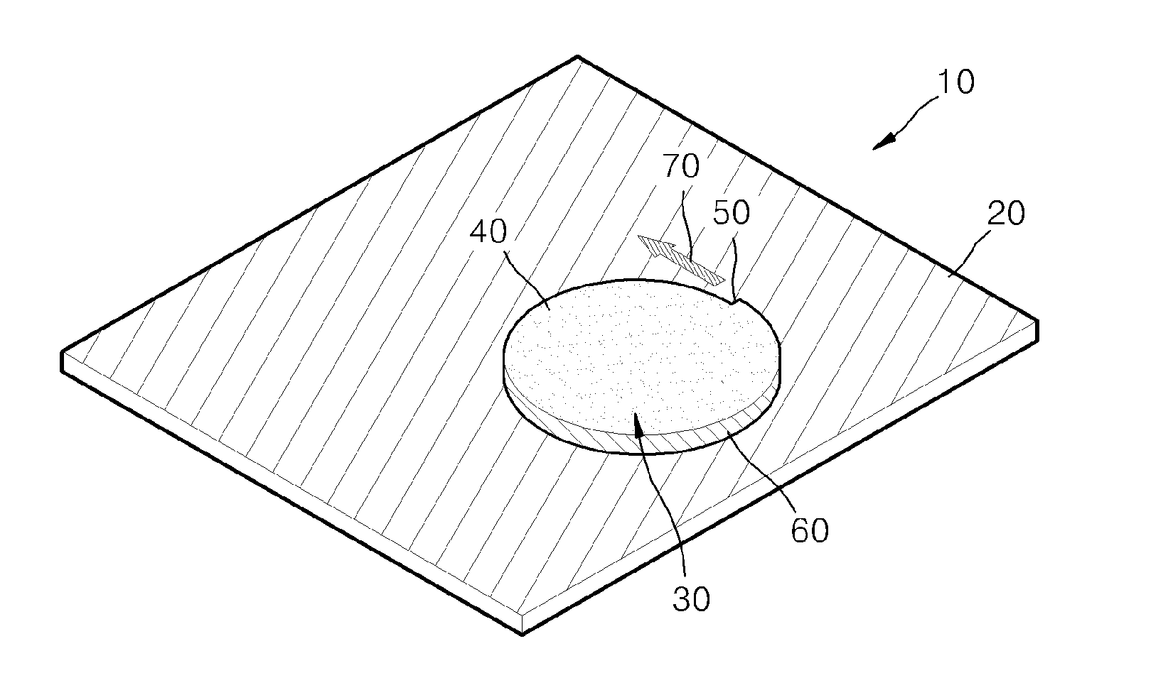
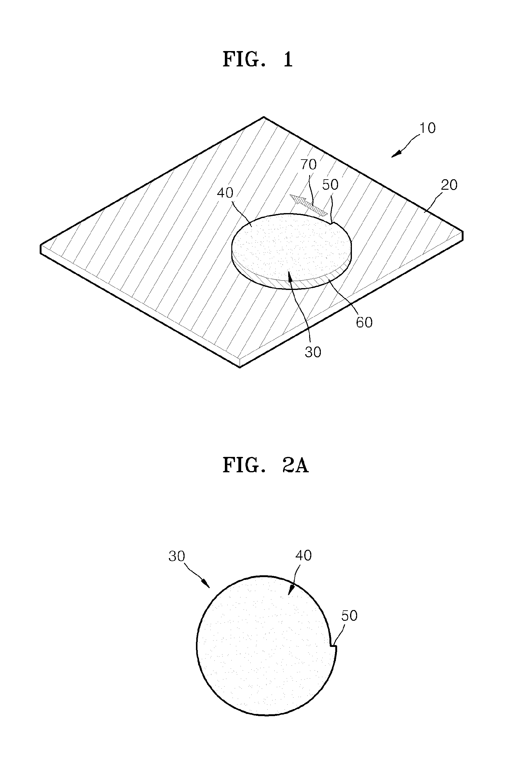
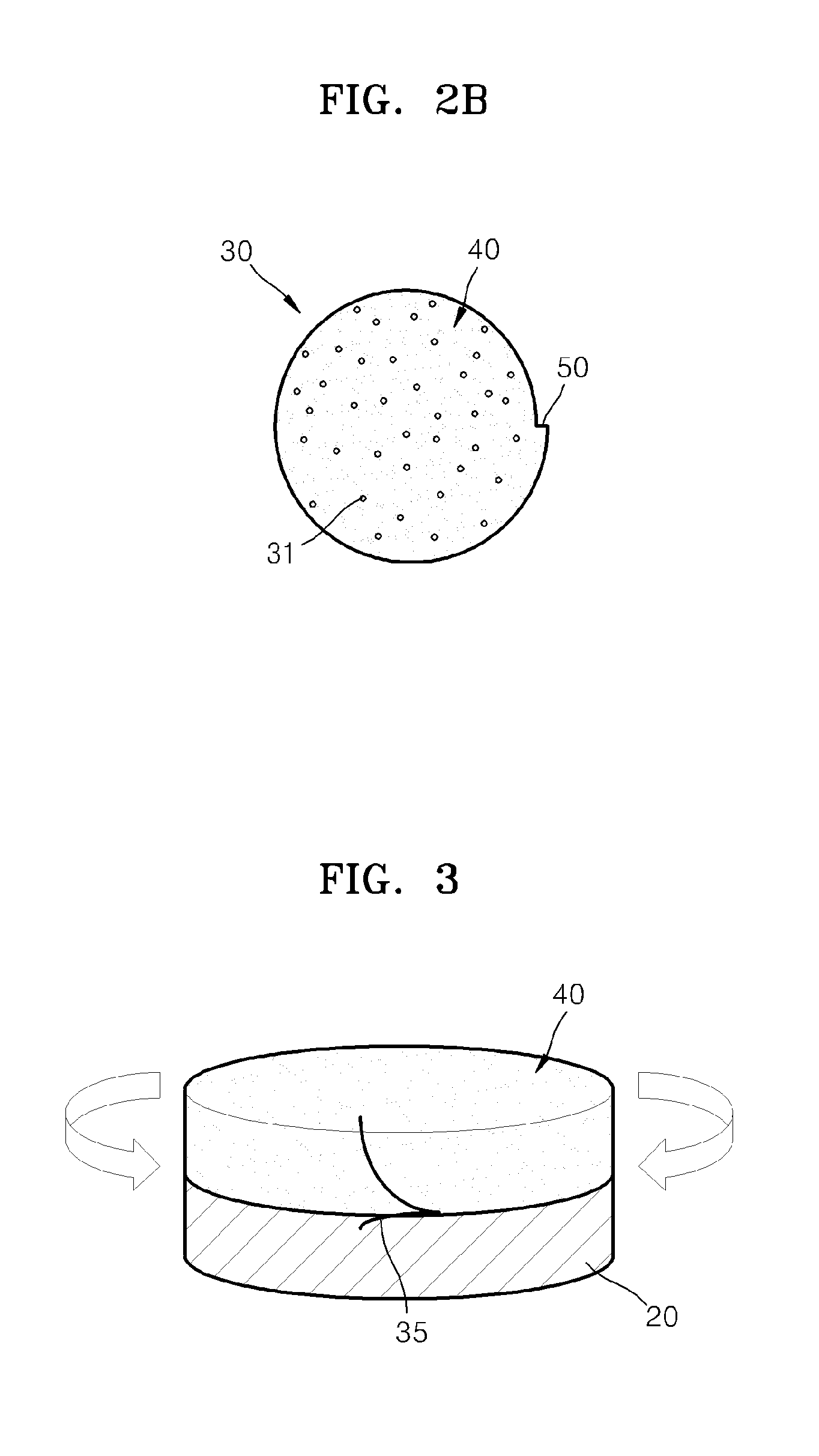
The patent describes a surface plasmon laser that generates a small laser beam with a high quality. The laser includes a metal layer, a gain medium layer, and a deformed portion through which the laser light is output. In one embodiment, the deformed portion is a notch formed in the gain medium layer. The laser light passes through a ring-shaped structure and a protruding guide before being output through a light guide. The surface plasmon laser has applications in optical sensing, imaging, and communication.

Problems solved by technology

However, there is a limit in the size of a small light spot in the lasers suggested thus far due to a limit in diffraction.

Method used


Image

  • Surface plasmon laser
  • Surface plasmon laser
  • Surface plasmon laser

Examples


Embodiment Construction

[0034]Reference will now be made in detail to embodiments, examples of which are illustrated in the accompanying drawings, wherein like reference numerals refer to like elements throughout. In this regard, the embodiments may have different forms and should not be construed as being limited to the descriptions set forth herein. Accordingly, the embodiments are merely described below, by referring to the figures, to explain aspects of the present description. As used herein, the term “and / or” includes any and all combinations of one or more of the associated listed items. Expressions such as “at least one of,” when preceding a list of elements, modify the entire list of elements and do not modify the individual elements of the list.

[0035]A surface plasmon laser according to exemplary embodiments is formed to embody a surface plasmon laser of a whispering gallery mode type in which surface plasmon light generated due to surface plasmon resonance rotates along a circle. To this end, th...


PUM


Abstract

A surface plasmon laser includes a metal layer, a gain medium layer provided on the metal layer and having a circular structure portion in which a whispering gallery mode is generated in which surface plasmon light generated due to surface plasmon resonance on an interface with the metal layer rotates along a circle, and a deformed portion formed to output part of laser light generated in the circular structure portion of the gain medium layer.

Description

CROSS-REFERENCE TO RELATED APPLICATIONS[0001]This application claims priority from Korean Patent Application No. 10-2011-0093643 filed Sep. 16, 2011, and Korean Patent Application No. 10-2012-0101625 filed Sep. 13, 2012, the disclosures of which are incorporated herein in their entirety by reference.BACKGROUND[0002]1. Field[0003]Embodiments relates to a laser, and more particularly, to a surface plasmon laser for oscillating laser light by using a surface plasmon resonance phenomenon.[0004]2. Description of the Related Art[0005]In general, optical integrated circuits are optical circuits on which various optical elements perform various operations such as light emission, optical detection, optical amplification, and optical modulation on a single substrate. For example, a light source, a photodetector, an optical waveguide, a lens, a grating, and an optical switch may be integrated on a single substrate. An optical integrated circuit may be diversely applied to devices in various fi...

Claims


Application Information

Patent Timeline
IPC IPC(8): H01S5/026
CPCH01S5/026H01S5/1046B82Y20/00H01S5/3412G02B6/1226H01S5/1075
Inventor LEE, JAE-SOONGKIM, UN-JEONGROH, YOUNG-GEUNPARK, YEON-SANG
Owner SAMSUNG ELECTRONICS CO LTD
Learn More