Method for manufacturing nitride semiconductor substrate

a manufacturing method and semiconductor technology, applied in the direction of polycrystalline material growth, crystal growth process, after-treatment details, etc., can solve the problems of poor yield rate, easy generation of cleavage, and large reduction of yield rate, so as to improve the yield rate of nitride semiconductor substrate and reduce cleavage

Active Publication Date: 2013-03-21
SUMITOMO CHEM CO LTD
View PDF27 Cites 7 Cited by
  • Summary
  • Abstract
  • Description
  • Claims
  • Application Information

AI Technical Summary

Benefits of technology

[0013]An object of the present invention is to provide a method for manufacturing a nitride semiconductor substrate capable of reducing a cleavage when slicing a nitride semiconductor single crystal and improving a yield rate of the nitride semiconductor substrate.

Problems solved by technology

However, when the crystal-grown GaN single crystal (ingot) is ground using a wire saw, cleavage is generated, resulting in a poor yield rate.
Particularly, when the GaN single crystal has a large diameter and when the GaN crystal is thick, the cleavage is easily generated and reduction of the yield rate is great.

Method used


Image

  • Method for manufacturing nitride semiconductor substrate
  • Method for manufacturing nitride semiconductor substrate
  • Method for manufacturing nitride semiconductor substrate

Examples


Embodiment Construction

[0024]Preferred embodiment of a method for manufacturing a nitride semiconductor substrate according to the present invention will be described hereafter.

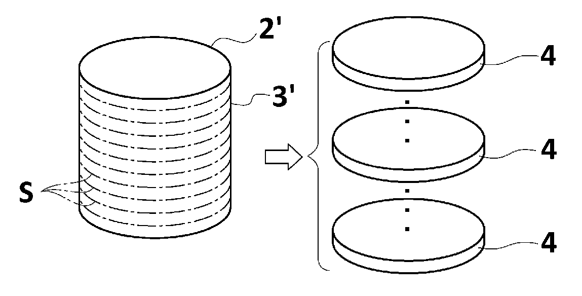
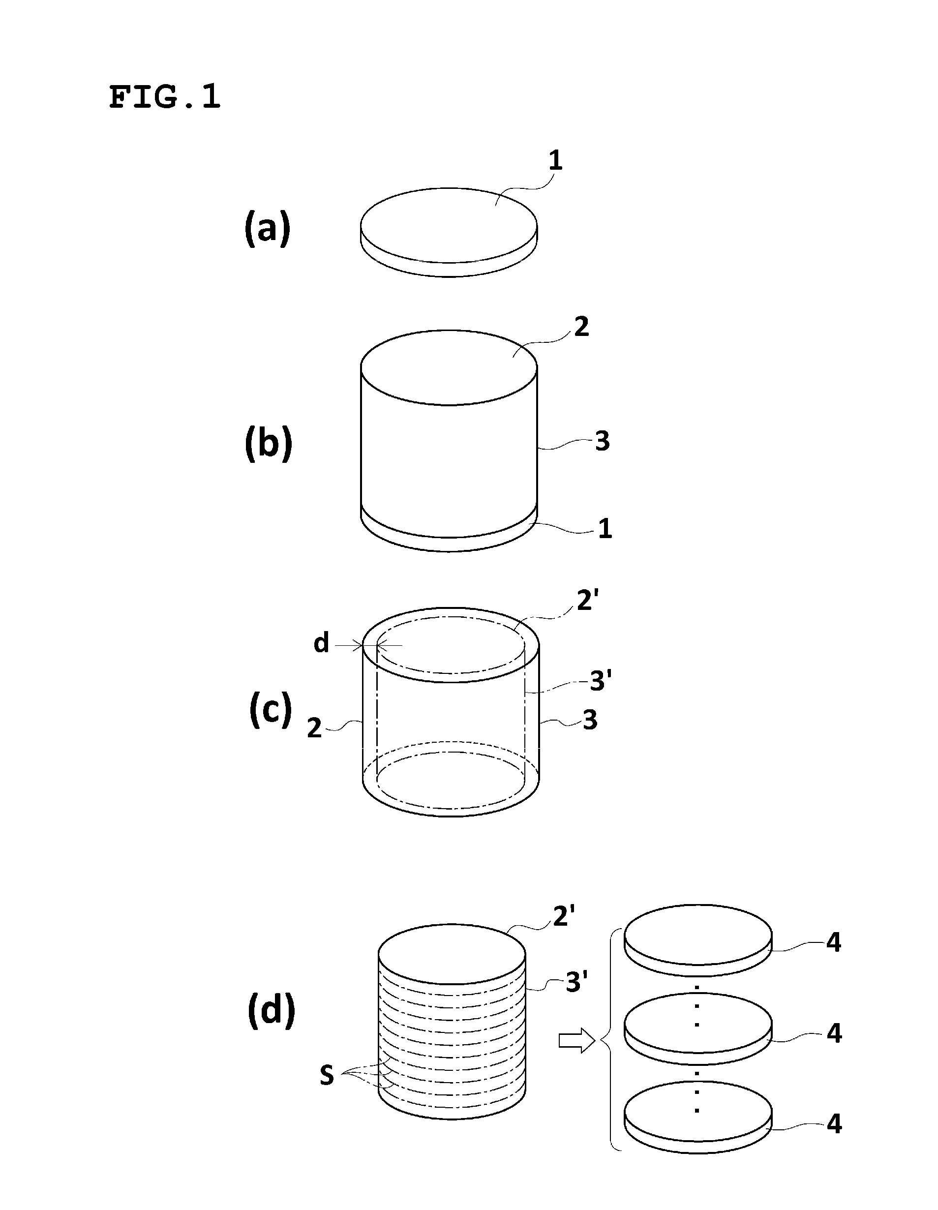
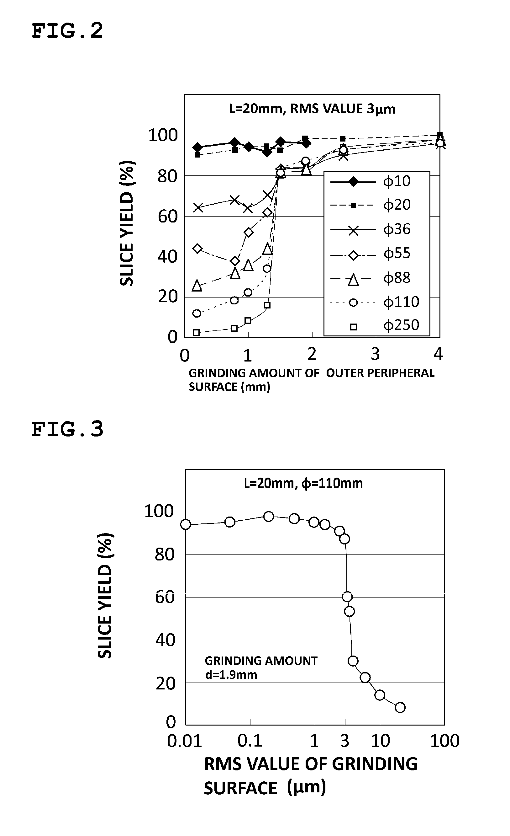
[0025]FIG. 1 is a step view of the method for manufacturing a nitride semiconductor substrate according to an embodiment of the present invention. In this embodiment, GaN is taken as an example of a nitride semiconductor for explanation.

[0026]First, a seed crystal substrate is prepared, for growing a GaN single crystal, being a nitride semiconductor single crystal. A disc-shaped GaN substrate (GaN freestanding substrate) 1 is used as the seed crystal substrate (FIG. 1(a)). A main surface of the disc-shaped GaN substrate 1 is taken as a C-plane, which is formed by a VAS method (a Void-Assisted Separation method) for example, or the GaN substrate manufactured by the method for manufacturing a nitride semiconductor substrate of the present invention may be used as the seed crystal substrate. The GaN substrate 1, being the seed crystal...


PUM

PropertyMeasurementUnit
diameteraaaaaaaaaa
surface roughnessaaaaaaaaaa
thicknessaaaaaaaaaa

Abstract

To provide a method for manufacturing a nitride semiconductor substrate capable of reducing a cleavage during slicing of a nitride semiconductor single crystal, and capable of improving a yield rate of the nitride semiconductor substrate, comprising: growing a nitride semiconductor single crystal on a seed crystal substrate by vapor phase epitaxy; grinding an outer peripheral surface of the grown nitride semiconductor single crystal; and slicing the nitride semiconductor single crystal with its outer peripheral surface ground, wherein a grinding amount of the outer peripheral surface of the nitride semiconductor single crystal in the step of grinding is 1.5 mm or more.

Description

BACKGROUND[0001]The present application is based on Japanese Patent Applications No. 2011-201491 filed on Sep. 15, 2011, the entire contents of which are hereby incorporated by reference.[0002]1. Technical Field[0003]The present invention relates to a method for manufacturing a nitride semiconductor substrate for manufacturing a plurality of nitride semiconductor substrates from a nitride semiconductor single crystal.[0004]2. Description of Related Art[0005]In order to fabricate a compound semiconductor substrate, there is a method of growing a compound semiconductor crystal (ingot) by a liquid-phase growth or a vapor-phase growth, then slicing an obtained ingot, to thereby fabricate a substrate (wafer).[0006]In a fabrication technique of the compound semiconductor substrate, for example, outer cylindrical grinding for grinding an outer periphery of the ingot is carried out, to remove impurities, etc., that exist on a skin of GaAs single crystal ingot before a wafer is fabricated by...

Claims


Application Information

Patent Timeline
Patent Type & Authority Applications(United States)
IPC IPC(8): H01L21/203
CPCC30B25/00C30B33/00C30B29/406
Inventor FUJIKURA, HAJIME
Owner SUMITOMO CHEM CO LTD
Why Eureka
Try Eureka