Semiconductor device and method for manufacturing semiconductor device

Active Publication Date: 2013-03-28
TOYOTA JIDOSHA KK +1
View PDF1 Cites 27 Cited by
  • Summary
  • Abstract
  • Description
  • Claims
  • Application Information

AI Technical Summary

Benefits of technology

[0037]Main trenches, a first termination trench and a second termination trench are formed simultaneously by the trench forming process. Insulating films are formed in the main trenches, the first termination trench and the second termination trench by the insulating film forming process. The width of the second termination trench is narrower than the first termination trench. Therefore, if the predetermined thickness of the insulating film is a thickness by which the second termination trench is fully filled by the insulating film and the first termination trench is not fully filled by the insulating layer, then it is possible to form the second termination t

Problems solved by technology

Therefore, it is possible to prevent concentration of the electric field in the termination region of th

Method used


Image

  • Semiconductor device and method for manufacturing semiconductor device
  • Semiconductor device and method for manufacturing semiconductor device
  • Semiconductor device and method for manufacturing semiconductor device

Examples


first embodiment

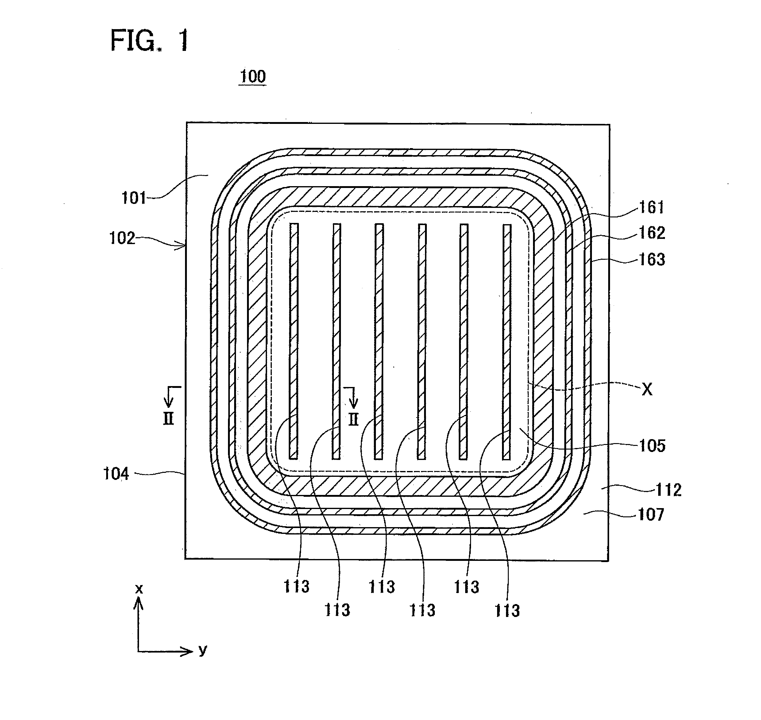
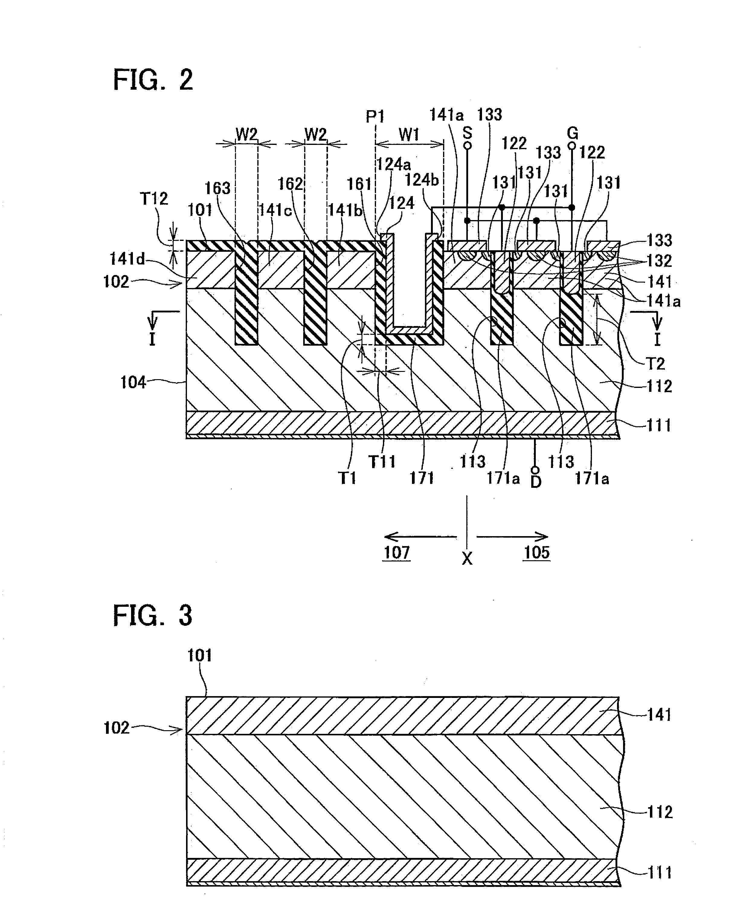
[0064]Below, a first embodiment of the semiconductor device which is a practical realization of the present teaching is described in detail with reference to the drawings. FIG. 1 is a plan diagram of the semiconductor device 100 according to the first embodiment. FIG. 2 is a cross-sectional diagram along line II-II in FIG. 1. More specifically, FIG. 1 corresponds to a cross-sectional diagram along line I-I in FIG. 2. In FIG. 1, the hatching relating to the drift region 112 is omitted.

[0065]As shown in FIG. 1, the semiconductor device 100 is manufactured by using a semiconductor substrate 102 having an outer circumference 104. The semiconductor substrate 102 is divided into a cell area 105 (inside the frame X indicated by the dotted lines in FIG. 1) in which a semiconductor structure performing a transistor operation is constructed, and a termination area 107 which surrounds this cell area 105.

[0066]The cell area 105 is formed in such a manner that six main trenches 113 extend in the...

second embodiment

[0100]A semiconductor device 100g relating to a second embodiment is now described in detail. As shown in FIG. 17, in the semiconductor device 100g, sidewalls and a bottom surface of a termination trench 161 are covered with an oxide film 171 and an interlayer insulating layer 172. Furthermore, upper portions of main trenches 113 are respectively covered with interlayer insulating layers 172b. A metal film 174 is formed so as to cover, in continuous fashion, a surface of the interlayer insulating layer 172 which covers the bottom surface and sidewalls of the termination trench 161, a surface of a body region 141a in a region to the inner circumference side of the termination trench 161, and surfaces of the interlayer insulating layers 172b which cover the main trenches 113. Furthermore, the metal film 174 is connected to a source electrode (not illustrated) and a source voltage is applied thereto. One example of the metal film174 is aluminum. It is also possible to use various other...

third embodiment

[0105]A semiconductor device 100b relating to a third embodiment is now described in detail. As shown in FIG. 12, in the semiconductor device 100b, sidewalls and a bottom surface of a termination trench 161 are covered with an oxide film 171. Furthermore, a buried electrode 124c is formed on a surface of the oxide film 171 which covers the sidewalls and bottom surface of the termination trench 161. The material of the buried electrode 124c is polysilicon. Furthermore, the buried electrode 124c is connected to a gate wire G.

[0106]The formation position of the buried electrode 124c is now described. An end portion 124d is formed in the buried electrode 124c. Here, when the semiconductor device 100b is observed from vertically above, the position of the surface of the oxide film 171 which covers the sidewall on the chip outer side (termination area 107 side) of the termination trench 161 is defined as position P2. The position of the end portion 124d is to the chip inner side of the po...


PUM


Abstract

The present application relates to technology for improving a withstand voltage of a semiconductor device. The semiconductor device includes a termination area that surrounds a cell area. The cell area is provided with a plurality of main trenches. The termination area is provided with one or more termination trenches surrounding the cell area. A termination trench is disposed at an innermost circumference of one or more termination trenches. A body region is disposed on a surface of a drift region. Each main trench reaches the drift region. A gate electrode is provided within each main trench. The termination trench reaches the drift region. Sidewalls and a bottom surface of the termination trench are covered with a insulating layer. A surface of the insulating layer covering the bottom surface of the termination trench is covered with a buried electrode. A gate potential is applied to the buried electrode.

Description

TECHNICAL FIELD[0001]This application claims priority to Japanese Patent Application No. 2010-133800 filed on 11 Jun. 2010 and Japanese Patent Application No. 2010-275477 filed on 10 Dec. 2010, the contents of which are hereby incorporated by reference into the present application. The present application relates to technology for improving a withstand voltage of a semiconductor device. In particular, the present application relates to technology for a semiconductor device using silicon carbide (hereinafter, abbreviated to SiC), whereby the withstand voltage can be raised in a semiconductor device having a cell area in which a semiconductor structure (for example, a MOSFET structure, an IGBT structure of a diode structure, etc.) is constructed, and a termination insulating region (termination area) which surrounds and broadens from the cell area.BACKGROUND ART[0002]Progress has been made in technology for constructing a semiconductor structure (MOSFET, IGBT, diode, etc.) which funct...

Claims


Application Information

Patent Timeline
IPC IPC(8): H01L29/16H01L29/49
CPCH01L29/0623H01L29/7397H01L29/0696H01L29/1608H01L29/407H01L29/41741H01L29/4236H01L29/42368H01L29/66068H01L29/7811H01L29/7813H01L21/046H01L29/49H01L29/0653H01L29/0619H01L29/0661
Inventor TAKAYA, HIDEFUMIMATSUKI, HIDEOSUZUKI, NAOHIROISHIKAWA, TSUYOSHI
Owner TOYOTA JIDOSHA KK
Why Eureka
Try Eureka