Semiconductor device and method for manufacturing the same

a technology of semiconductor devices and semiconductor devices, applied in the direction of semiconductor devices, basic electric elements, electrical appliances, etc., can solve the problems of inability to contribute to improving the defect of crystals cannot be sufficiently effective life killers, so as to improve the characteristics of semiconductor devices

Inactive Publication Date: 2013-03-28
TOYOTA JIDOSHA KK
View PDF20 Cites 61 Cited by
  • Summary
  • Abstract
  • Description
  • Claims
  • Application Information

AI Technical Summary

Benefits of technology

[0009]In the semiconductor device described above, the crystal defects in the lifetime control region are formed by the hydrogen ions irradiated when forming the high impurity n layer. Therefore, the donor peak position, at which the hydrogen ion donor density is the highest in the high impurity n layer in the depth direction of the semiconductor substrate, is adjacent or identical to the defect peak position, at which the crystal defect density is the highest in the lifetime control region in the depth direction of the semiconductor substrate. In addition, the crystal defect density in the defect peak position of the lifetime control region is 1×10¹² atoms / cm3 or more, and has the crystal defect density distribution that enables the characteristics of the semiconductor device to be improved. According to the semiconductor device described above, the lifetime control region that is effective in improving the characteristics of the semiconductor device can be formed by utilizing the process of manufacturing the high impurity n layer.

Problems solved by technology

Therefore, the crystal defects cannot sufficiently function as a lifetime killer and are unable to contribute to improving characteristics of a semiconductor device.

Method used


Image

  • Semiconductor device and method for manufacturing the same
  • Semiconductor device and method for manufacturing the same
  • Semiconductor device and method for manufacturing the same

Examples


first embodiment

[0041](Semiconductor Device)

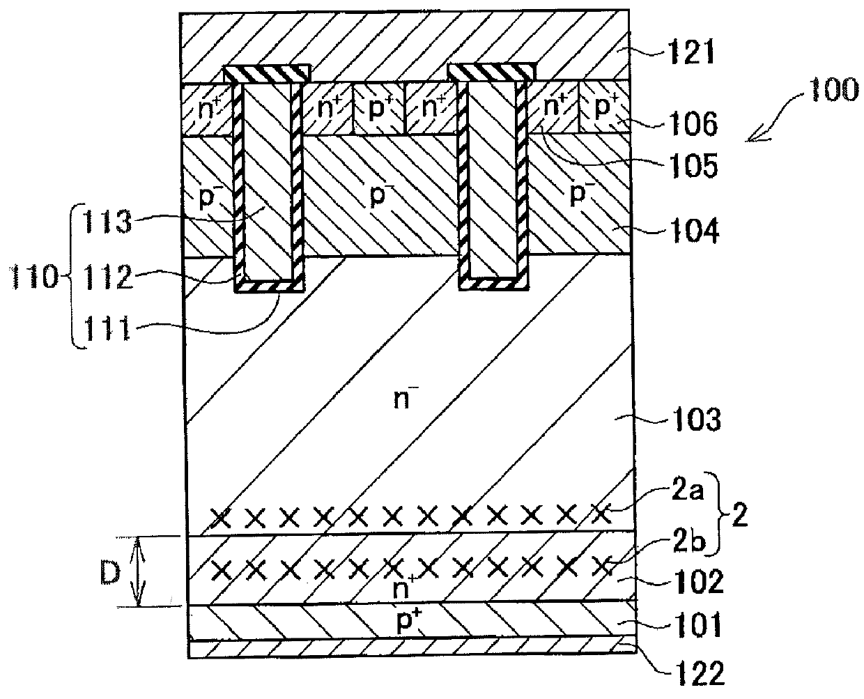
[0042]A semiconductor device 10 shown in FIG. 1 is an IGBT comprising a buffer layer 102 as a high impurity n layer. The semiconductor device 10 comprises a semiconductor substrate 100, an emitter electrode 121 provided on an upper surface of the semiconductor substrate 100, and a collector electrode 122 provided on a lower surface of the semiconductor substrate 100. The IGBT is formed on the semiconductor substrate 100. The semiconductor substrate 100 comprises, in order from the lower surface side of the semiconductor substrate 100, a p type collector layer 101, an n type buffer layer 102, an n type drift layer 103, a p type body layer 104, n type emitter layers 105 and a p type body contact layer 106. The emitter layers 105 and the body contact layer 106 are isolated from the drift layer 103 by the body layer 104. The semiconductor substrate 100 further comprises insulated gates 110 in contact with the body layer 104 that is positioned between the emit...

second embodiment

[0067]The semiconductor device according to the present teachings is not limited to the IGBT and may instead be a diode, a MOSFET, an RC-IGBT, or the like. As one alternative example, a semiconductor device 50 shown in FIG. 23 will be described. The semiconductor device 50 is an RC-IGBT comprising a buffer layer 502 and a cathode layer 531 as a high impurity n layer. The semiconductor device 50 comprises a semiconductor substrate 500, an upper surface electrode 521 provided on an upper surface of the semiconductor substrate 500, and a lower surface electrode 522 provided on a lower surface of the semiconductor substrate 500. An IGBT and a diode are formed on the semiconductor substrate 500. The semiconductor substrate 500 comprises, in order from the lower surface side of the semiconductor substrate 500, a p type collector layer 501 and an n type cathode layer 531, an n type buffer layer 502, an n type drift layer 503, a p type body layer 504, and n type emitter layers 505 and a p t...


PUM


Abstract

A semiconductor device includes: a semiconductor substrate, the semiconductor substrate comprising; an n type drift layer, a p type body layer on an upper surface side of the drift layer, and a high impurity n layer on a lower surface side of the drift layer. The high impurity n layer includes hydrogen ion donors as a dopant, and has a higher density of n type impurities than the drift layer. A lifetime control region including crystal defects as a lifetime killer is formed in the high impurity n layer and a part of the drift layer. A donor peak position is adjacent or identical to a defect peak position, at which a crystal defect density is highest in the lifetime control region in the depth direction of the semiconductor substrate. The crystal defect density in the defect peak position of the lifetime control region is 1×10¹² atoms/cm3 or more.

Description

CROSS-REFERENCE TO RELATED APPLICATION[0001]This application claims priority to Japanese Patent Application No. 2011-213006 filed on Sep. 28, 2011, the contents of which are hereby incorporated by reference into the present application.TECHNICAL FIELD[0002]The present teachings relate to a semiconductor device and a method of manufacturing the same.DESCRIPTION OF RELATED ART[0003]In semiconductor devices, a region (in the present specification, hereinafter referred to as a lifetime control region) having a locally formed crystal defect is sometimes formed on a semiconductor substrate in order to control a lifetime of a carrier. For example, Japanese Patent Application Publication No. H9-121052 discloses a technique for forming a lifetime control region in a drift layer or a collector layer of an insulated gate-type bipolar transistor (IGBT) in order to reduce both a turn-off time and a turn-off loss of the IGBT. The lifetime control region is formed by implanting light ions such as ...

Claims


Application Information

Patent Timeline
Patent Type & Authority Applications(United States)
IPC IPC(8): H01L21/265H01L29/739
CPCH01L21/263H01L29/36H01L29/0834H01L29/66348H01L29/7397H01L29/861H01L29/32
Inventor YAMAZAKI, SHINYAKAMEYAMA, SATORUSAKANE, HITOSHIITO, JYOJI
Owner TOYOTA JIDOSHA KK
Why Eureka
Try Eureka