Far infrared ray ceramic bulb structure
a ceramic bulb and infrared ray technology, applied in the direction of gas-filled discharge tubes, semiconductor devices of light sources, lighting and heating apparatus, etc., can solve the problems of low whole energy conversion efficiency, or specifically much less than 50%, serious safety problems, and limited practical application, so as to improve stability and light-emitting efficiency, reduce the working temperature of light-emitting elements, and increase the lifetime and safety
- Summary
- Abstract
- Description
- Claims
- Application Information
AI Technical Summary
Benefits of technology
Problems solved by technology
Method used
Image
Examples
first embodiment
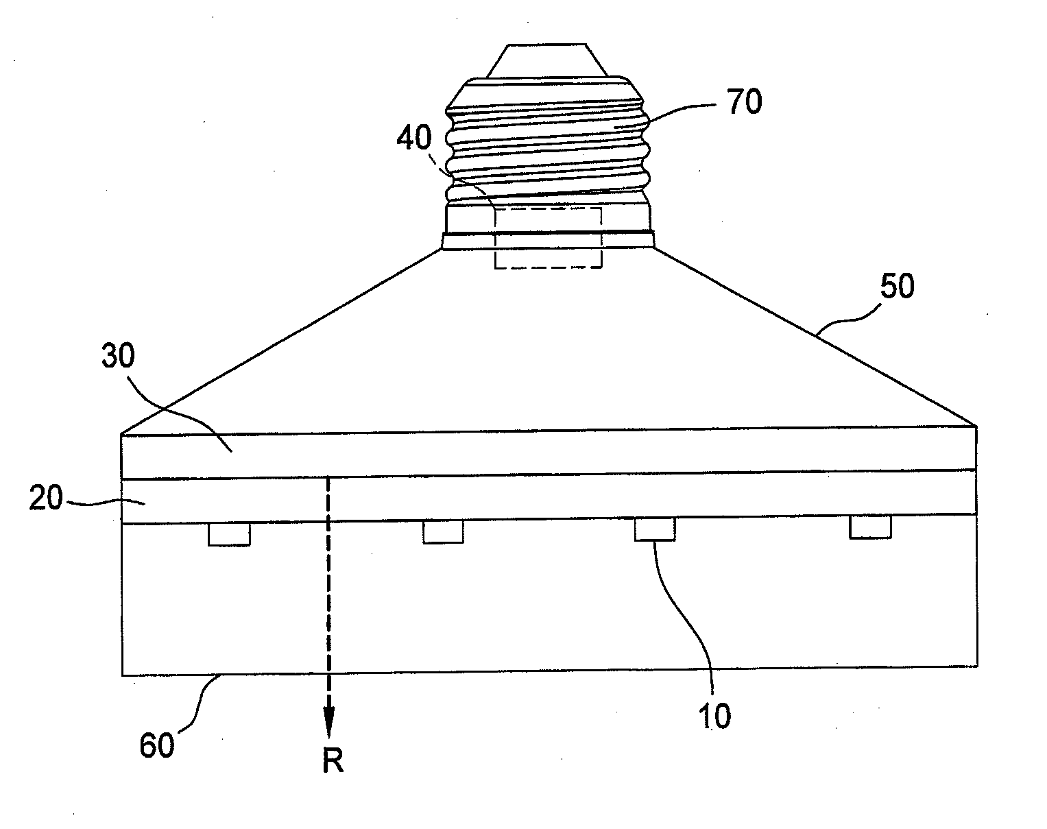
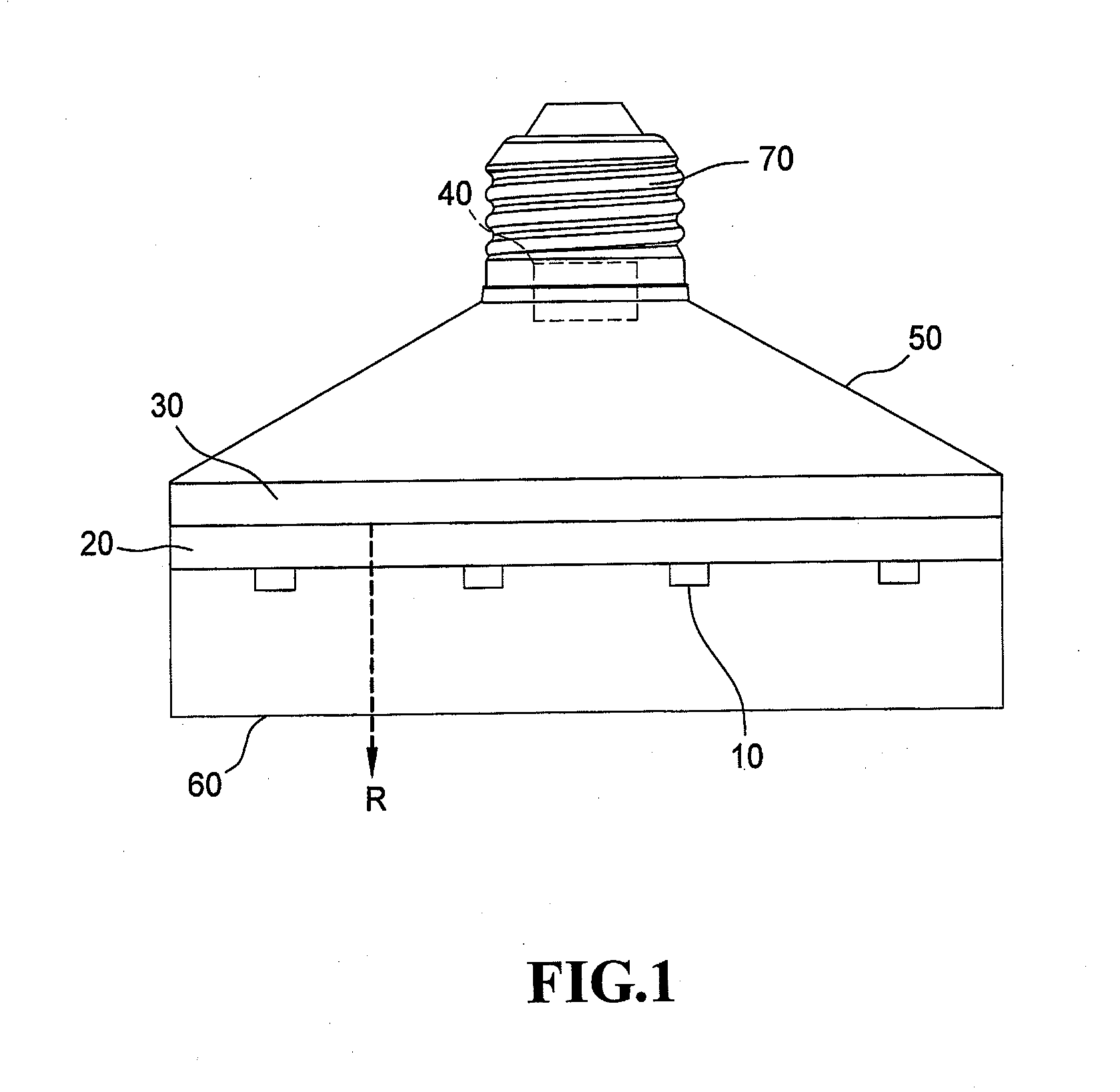
[0018]FIG. 1 clearly illustrates a far infrared ray ceramic bulb structure according to the present invention, and includes a light emitting element 10, a ceramic substrate 20, a far infrared thermal radiation film 30, a circuit unit 40, a bulb shell 50, a bulb shade 60 and a connector 70. The far infrared ray ceramic bulb structure of the present invention uses the light emitting element 10 to produce light, and the far infrared thermal radiation film 30 to emit far infrared ray R, which has a wavelength primarily within the range of 4 to 400 μm, and especially 6 to 14 μm.
[0019]The light emitting element 10 consists of an LED (light emitting diode) chip.
[0020]The ceramic substrate 20 has an upper surface and a lower surface. The light emitting element 10 is formed on a sapphire substrate (not shown) and is connected to the lower surface of the ceramic substrate 20. The far infrared thermal radiation film 30 is formed on the upper surface of the ceramic substrate 20. The circuit uni...
second embodiment
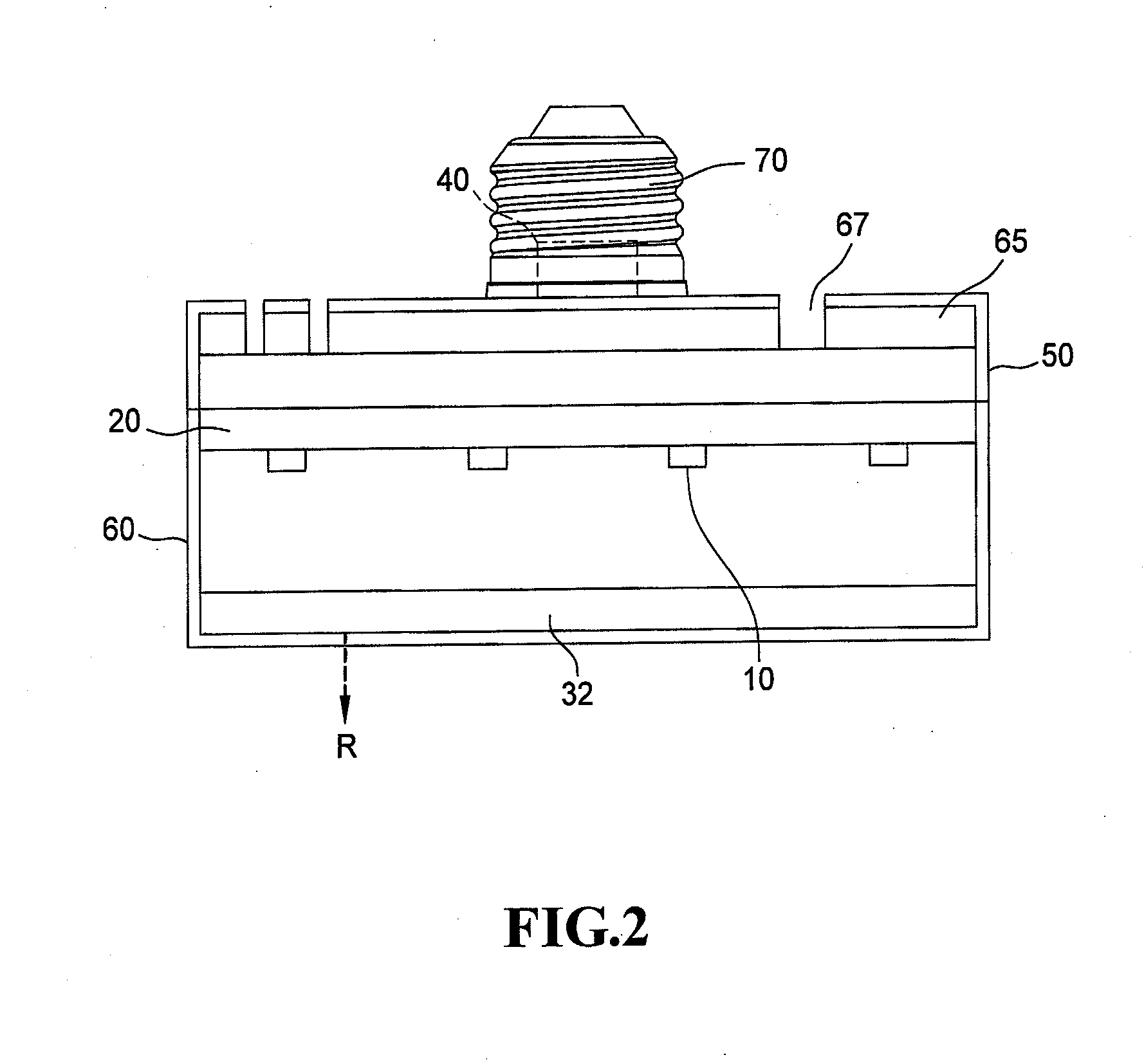
[0026]FIG. 2 illustrates the far infrared ray ceramic bulb structure according to the present invention. As shown in FIG. 2, the far infrared ray ceramic bulb structure of the present invention includes the LED chip 10, the ceramic substrate 20, the far infrared thermal radiation film 32, the circuit unit 40, the bulb shell 50, the bulb shade 60, the nano-enamel heat dissipation cover 65 and the connector 70. The far infrared ray ceramic bulb structure uses the LED chip 10 to emit light and the far infrared thermal radiation film 32 to generate far infrared ray R.
[0027]The far infrared ray ceramic bulb structure in FIG. 2 is similar to the first embodiment of the far infrared ray ceramic bulb structure, and the primary difference is that the far infrared thermal radiation film 32 is formed on the upper surface of the bulb shade 60, that is, the upward surface in FIG. 2.
[0028]Another difference is that the bulb shell 50 is connected to the connector 70 and encloses the upper surface ...
fourth embodiment
[0033]As shown in FIG. 5, the far infrared ray ceramic bulb structure according to the present invention includes the LED chip 10, the ceramic substrate 20, the far infrared thermal radiation film 30, the circuit unit 40, the bulb shell 50, the bulb shade 60 and the connector 70. The far infrared ray ceramic bulb structure uses the LED chip 10 to emit light and the far infrared thermal radiation film 30 generates far infrared ray R with a wavelength within the range of 4 to 400 μm, and especially 6 to 14 μm.
[0034]The far infrared ray ceramic bulb structure in FIG. 5 is similar to the far infrared ray ceramic bulb structure of the first embodiment in FIG. 1. The primary difference between the fourth and first embodiments is that the far infrared thermal radiation film 30 of the fourth embodiment is formed under the ceramic substrate 20 and on the LED chip 10, and the heat generated by the circuit unit 40 is directly transferred downwards by far infrared thermal radiation R direction....
PUM
| Property | Measurement | Unit |
|---|---|---|
| temperature | aaaaa | aaaaa |
| temperature | aaaaa | aaaaa |
| temperature | aaaaa | aaaaa |
Abstract
Description
Claims
Application Information


