System and method for reducing cross coupling effects

Inactive Publication Date: 2013-03-28
QUALCOMM INC
View PDF4 Cites 9 Cited by
  • Summary
  • Abstract
  • Description
  • Claims
  • Application Information

AI Technical Summary

Benefits of technology

[0006]In a particular embodiment, a device may include a plurality of driver circuits coupled to a plurality of bus lines. A first driver circuit of the plurality of driver circuits may be coupled to a first bus line of the plurality of bus lines. The first driver circuit may include a delay element configured to produce an output signal. The output signal may transition after a first delay in response to a first digital value transition of an input signal from high to low and may transition after a second delay in response to a second digital value transition of the input signal from low to high. The first delay may be different from the second delay by an amount sufficient to reduce power related to transmission of signals over the first bus line and over a second bus line in close physical proximity to the first bus line. For example, the delay element may prevent signals on the first and second bus lines from switching at the same time, potentially reducing the energy required to switch the bus lines. The delay element may include a skewed inverter, a level shifter, a latch, or a sense amplifier. In addition, a second driver circuit including the delay element may be coupled to the second bus line (i.e., the second bus line may also include the delay element). Further, in a particular illustrative implementation, all of the plurality driver circuits coupled to the plurality of bus lines may include the delay element.
[0007]In another particular embodiment, a method may include receiving a first input signal at a delay element coupled to a first bus line of a plurality of bus lines. The first input signal has a first digital value transition from high to low. The method further includes generating a first output signal at the delay element in response to the first input signal, where the first output signal transitions after a first delay. The method further includes receiving a second input signal at the delay element. The second input signal has a second digital value transition from low to high. The method further includes generating a second output signal a

Problems solved by technology

As electronic devices such as wireless telephones become smaller, there may be a tradeoff between scaling technology and power dissipation of on-chip buses in the electronic devices.
However, this may not effectively address the increased power dissipation because line to line capacitance may still occur at supply nodes of the bus lines.
However, increasing the spacing between bus lines may result in an unacceptable increase in die area.
H

Method used


Image

  • System and method for reducing cross coupling effects
  • System and method for reducing cross coupling effects
  • System and method for reducing cross coupling effects

Examples


Embodiment Construction

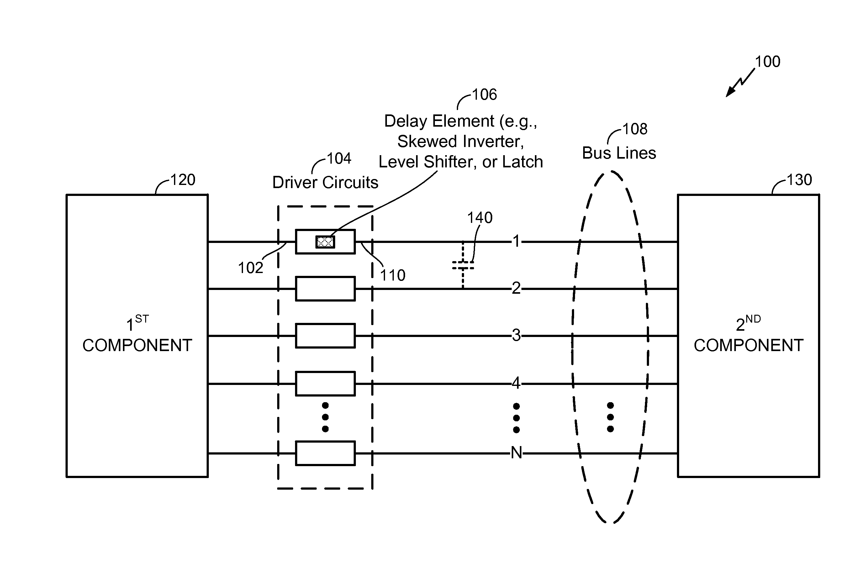
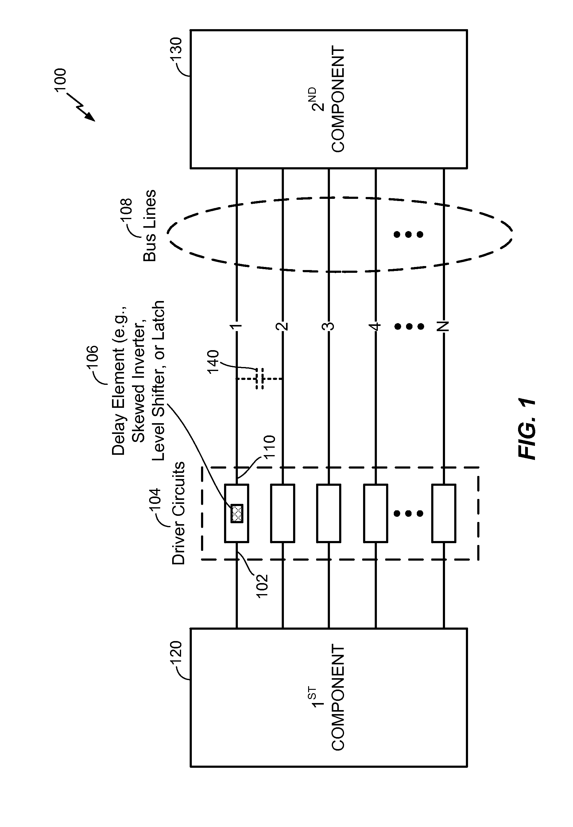
[0021]Referring to FIG. 1, a particular illustrative embodiment of a system to reduce cross coupling effects on bus lines is disclosed and generally designated 100. The system 100 includes a first component 120 coupled to a second component 130 via a plurality of bus lines 108. Each of the bus lines 108 may be coupled to one of a plurality of driver circuits 104.

[0022]In an illustrative embodiment, the first component 120 and the second component 130 are hardware components that are integrated into an electronic device, such as a wireless telephone. For example, the first component 120 and the second component 130 may include components of the electronic device described with reference to FIG. 10.

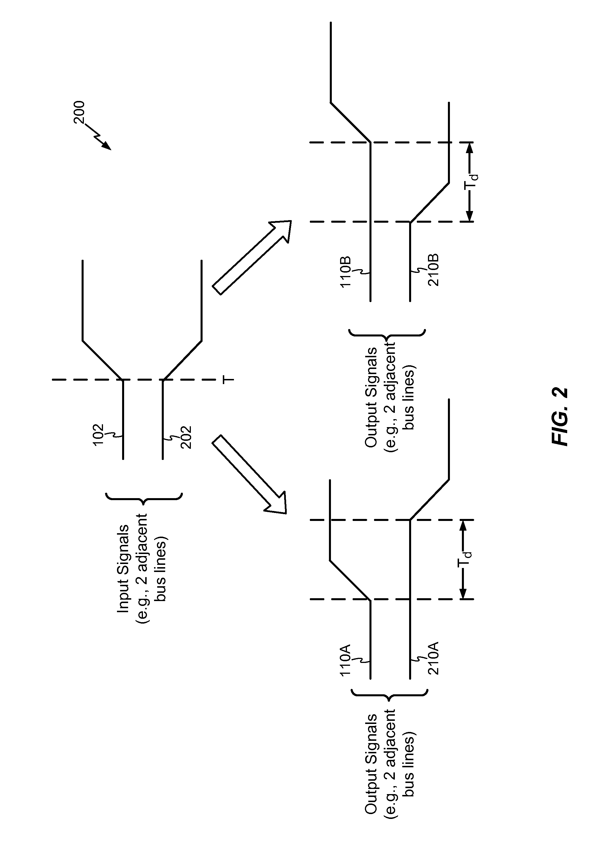
[0023]A first driver circuit of the plurality of driver circuits 104 may be coupled to a first bus line (designated “1” in FIG. 1) of the plurality of bus lines 108. The first driver circuit may include a delay element 106, receive an input signal 102, and produce an output signal 110. The ...


PUM


Abstract

A device includes a plurality of driver circuits coupled to a plurality of bus lines. A first driver circuit of the plurality of driver circuits is coupled to a first bus line of the plurality of bus lines. The first driver circuit includes one of a skewed inverter, a level shifter, a latch, and a sense amplifier configured to produce an output signal that transitions after a first delay in response to a first digital value transition of an input signal from high to low and transitions after a second delay in response to a second digital value transition of the input signal from low to high. The first delay is different from the second delay by an amount sufficient to reduce power related to transmission of signals over the first bus line and over a second bus line in close physical proximity to the first bus line.

Description

I. FIELD[0001]The present disclosure is generally related to reducing cross coupling effects.II. DESCRIPTION OF RELATED ART[0002]Advances in technology have resulted in smaller and more powerful computing devices. For example, there currently exist a variety of portable personal computing devices, including wireless computing devices, such as portable wireless telephones, personal digital assistants (PDAs), and paging devices that are small, lightweight, and easily carried by users. More specifically, portable wireless telephones, such as cellular telephones and internet protocol (IP) telephones, can communicate voice and data packets over wireless networks. Further, many such wireless telephones include other types of devices that are incorporated therein. For example, a wireless telephone can also include a digital still camera, a digital video camera, a digital recorder, and an audio file player. Also, such wireless telephones can process executable instructions, including softwa...

Claims


Application Information

Patent Timeline
IPC IPC(8): H03H11/26
CPCH03K3/356069Y02B60/1235Y02B60/1228G06F13/4072G06F13/4077G06F13/4291H03K5/15Y02D10/00G06F3/00G06F13/28H03K3/356113
Inventor MOHAMMAD, BAKER S.BASSETT, PAUL D.SAINT-LAURENT, MARTIN
Owner QUALCOMM INC
Why Eureka
Try Eureka