Semiconductor integrated circuit device

Inactive Publication Date: 2010-07-29
RENESAS ELECTRONICS CORP
View PDF8 Cites 1 Cited by
  • Summary
  • Abstract
  • Description
  • Claims
  • Application Information

AI Technical Summary

Benefits of technology

[0017]According to the above-mentioned embodiment, all operations are performed at 1.2 V during a normal operation, and power supply voltage is reduced to 0.8 V in a preset operation state, whereby it is possible to reduce power of main logic c

Problems solved by technology

Moreover, driving voltage becomes reduced along with the advance of technology, which results in a further increase in fluctuations of device characteristics which result from variations in PVT.
Under the circumstances, a limitation is being posed on scaling of a threshold value in a bulk silicon device, and hence it is difficult to

Method used


Image

  • Semiconductor integrated circuit device
  • Semiconductor integrated circuit device
  • Semiconductor integrated circuit device

Examples


first embodiment

A. First Embodiment

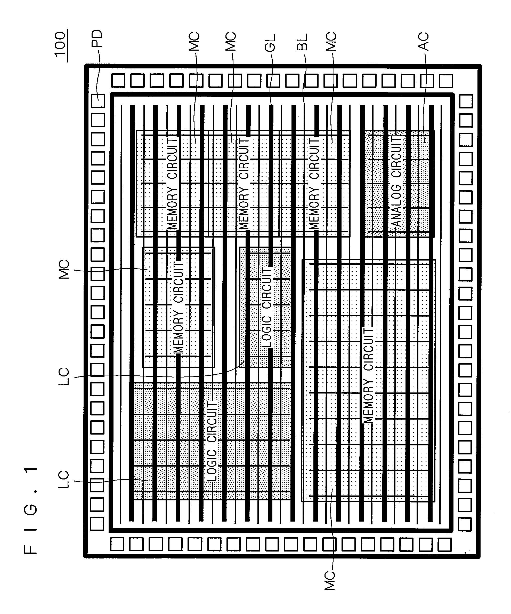
[0045]FIG. 1 is a view showing a layout in plan view of a semiconductor integrated circuit device 100 according to a first embodiment of the present invention.

[0046]As shown in FIG. 1, the semiconductor integrated circuit device 100 includes a plurality of logic circuits LC, an analog circuit AC, and a plurality of memory circuits MC, which are disposed on the same chip, and a plurality of pad electrodes PD are disposed along an edge of the chip so as to surround those. The plurality of pad electrodes PD are broadly classified into ones for supplying power supply voltage from the outside, ones for controlling body voltage, and ones which serve as a signal input portion.

[0047]The logic circuit LC is equipped with a central processing unit (CPU), various intellectual properties corresponding to uses such as image processing and network processing, while the analog circuit AC is equipped with an analog / digital converter, a digital / analog converter, an interface circu...

second embodiment

B. Second Embodiment

[0084]FIG. 13 is a block diagram showing a configuration of a self-correcting reference voltage generating circuit 200 according to a second embodiment of the present invention.

[0085]The self-correcting reference voltage generating circuit 200 mainly includes body control oscillators 1 and 2, a phase comparator 3, a charge pump 5, a loop filter 6 and a reference voltage generating circuit 7 (correction circuit), and the phase comparator 3, the charge pump 5 and the loop filter 6 constitute a so-called phase-locked loop (PLL) circuit.

[0086]Outputs of the body control oscillators 1 and 2 are respectively fed back to inputs thereof, and are also input to input portions IN1 and IN2 of the phase comparator 3 as internal oscillation clocks CLK1 and CLK2, respectively. The phase comparator 3 compares phases thereof and, in a case where there is a gap therebetween, outputs an up signal (up) and a down signal (down) as pulse signals for eliminating the gap.

[0087]The charg...

third embodiment

C. Third Embodiment

[0105]FIG. 14 is a block diagram showing a configuration of a self-correcting reference voltage generating circuit 300 according to a third embodiment of the present invention. Note that the same configurations as those of the self-correcting reference voltage generating circuit 200 shown in FIG. 13 are denoted by the same reference symbols, and overlapping description will be omitted.

[0106]The self-correcting reference voltage generating circuit 300 compares the phases of the internal oscillation clocks CLK 1 and CLK2, which are output from the body control oscillators 1 and 2, respectively, by the phase comparator 3 and, in a case where there is the gap between the phases thereof, performs an operation to output an up signal and a down signal for eliminating the gap as a pulse signal correct the reference voltages VP and VN corresponding to the body control voltage by a reference voltage generating circuit 7A (correction circuit) to supply them to the body contr...


PUM


Abstract

The present invention provides a semiconductor integrated circuit device in which characteristics of an SOI transistor are effectively used to achieve higher speed, higher degree of integration, and also reduction in voltage and power consumption. The semiconductor integrated circuit device according to the present invention has a configuration in which a plurality of external power supply lines and body voltage control lines are alternately arranged in one direction so as to extend over the entire chip, which supply power and a body voltage to logic circuits, an analog circuit and memory circuits. A body voltage control type logic gate is fully applied in the logic circuit, whereas the body voltage control type logic gate is partially applied in the memory circuit.

Description

RELATED APPLICATIONS[0001]This application is the U.S. National Phase under 35 U.S.C. §371 of International Application No. PCT / JP2008 / 067011, filed on Sep. 19, 2008, which in turn claims the benefit of Japanese Application No. 2007-257068, filed on Oct. 1, 2007, the disclosures of which Applications are incorporated by reference herein.TECHNICAL FIELD[0002]The present invention relates to a semiconductor integrated circuit device, and more particularly, to a semiconductor integrated circuit device having a low-voltage power down mode and a normal operation mode.BACKGROUND ART[0003]In recent years, the microprocessing technology is progressing for achieving higher speed and higher degree of integration of a semiconductor integrated circuit device. Along with this, variations in process, voltage and temperature (PVT) affect device characteristics more remarkably, and accordingly the technology of controlling an influence on the characteristics in an entire circuit against such variat...

Claims


Application Information

Patent Timeline
IPC IPC(8): H03K19/0944
CPCH01L27/088H01L27/108H01L27/10802H01L29/78615H01L27/1203H01L29/7841H01L27/10844H10B12/20H10B12/01H10B12/00
Inventor MORISHITA, FUKASHI
Owner RENESAS ELECTRONICS CORP
Why Eureka
Try Eureka