

Resist developer, method for forming a resist pattern and method for manufacturing a mold
a technology of resist developer and resist pattern, which is applied in the direction of photosensitive material processing, photomechanical equipment, instruments, etc., can solve the problems of increasing the demand for recording density, and the inability to ignore the magnetic influence between adjacent tracks, so as to achieve high resolution
- Summary
- Abstract
- Description
- Claims
- Application Information
AI Technical Summary
Benefits of technology
Problems solved by technology
Method used
Image

Examples
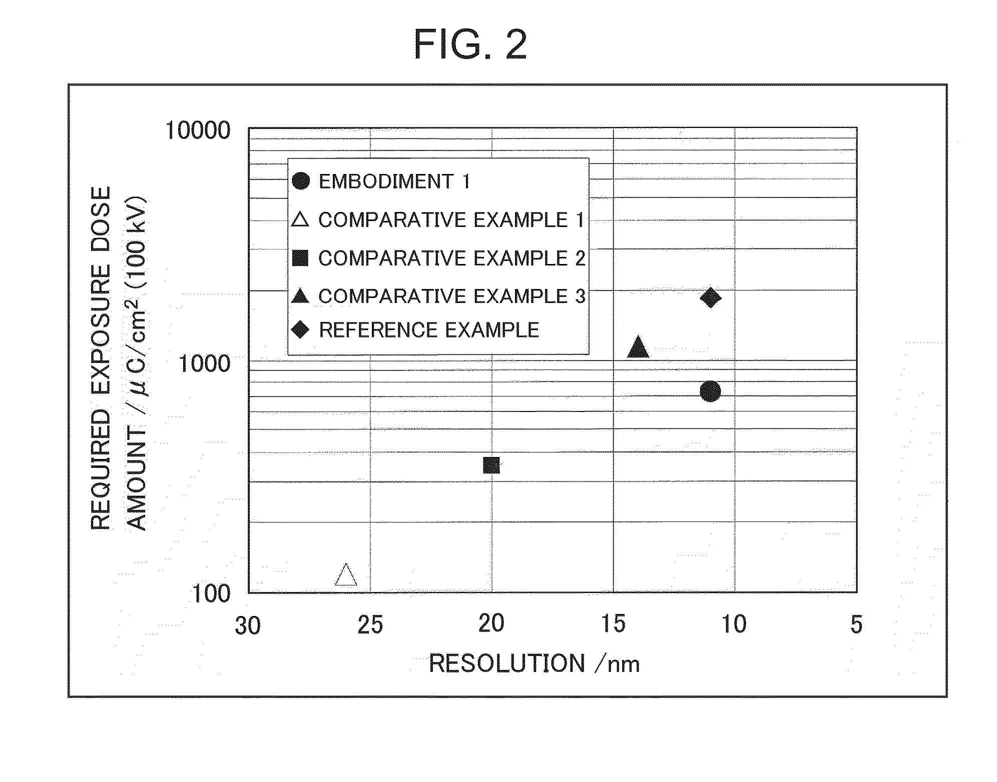
embodiment 1
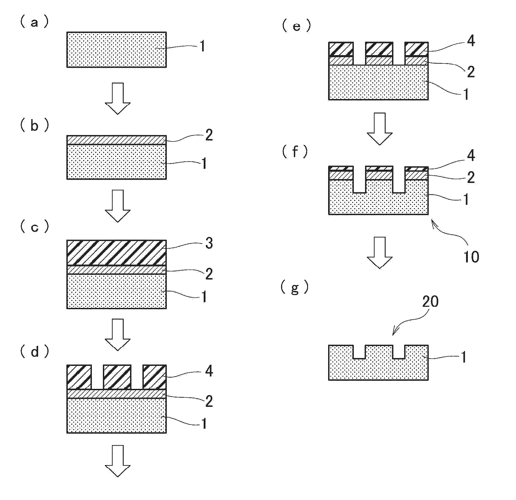
[0101]In the present embodiment, a wafer-shaped synthesized quartz substrate (150 mm in outer diameter and 0.7 mm in thickness) was used (FIG. 1(a)) as a substrate 1.
[0102]First, the substrate 1 is introduced into the sputtering apparatus, and a target made of chromium (Cr) is sputtered by argon gas and nitrogen gas to form the hard mask layer 2 made up of chromium nitride having a thickness of 2 nm (FIG. 1(b)). Baking was carried out for the substrate 1 on which the hard mask layer is formed, on a hot plate at 200° C. for 10 minutes in order to perform a dehydration bake process. Subsequently, the substrate 1 was placed on a cooling plate that is kept at a room temperature (22.5° C.), to cool the substrate 1.
[0103]Next, the substrate 1 on which the hard mask layer is formed was placed on a resist coater. Then, ZEP520A-7 (manufactured by Zeon Corporation), which is the polymer of α-chloromethacrylate and α-methylstyrene, was diluted with ZEP-A (manufactured by Zeon Corporation), whi...
embodiments 2 to 5
[0110]In the embodiment 1, the volume mixing ratio of the solvent A to the solvent B was 5 to 3, that is, the volume mixing ratio of the solvent B to (solvent A+solvent B) was 37.5%. In contrast, in the embodiments 2 to 5, the volume mixing ratio of the solvent B to (solvent A+solvent B) was varied to 10%, 25%, 50%, and 75%. As with the embodiment 1 except for the ratio, a sample was similarly manufactured. As a reference example, a sample having the ratio of 0% was also manufactured. A sample having the ratio of 100% corresponds to a comparative example 3 described later.
Reference Example
[0111]The following sample that shows remarkable effects of the embodiment and not disclosed yet was manufactured as a reference example based on the knowledge obtained by the inventors so far. That is, the reference example was prepared as with the embodiment 1 except that the developer was made up of only Vertrel XF instead of the mixed solution of Vertrel XF and isopropanol in the embodiment.
PUM
 Abstract
Description
Claims
Application Information