Component built-in wiring board and manufacturing method of component built-in wiring board

a manufacturing method and technology of component, applied in the direction of printed circuit, sustainable manufacturing/processing, final product manufacturing, etc., can solve the problems of reducing the productivity of components, and reducing the efficiency of components, so as to achieve low cost, high productivity, and low cost

Inactive Publication Date: 2013-04-04
DAI NIPPON PRINTING CO LTD
View PDF5 Cites 0 Cited by
  • Summary
  • Abstract
  • Description
  • Claims
  • Application Information

AI Technical Summary

Benefits of technology

[0015]The present invention relates to a component built-in wiring board having components buried and mounted in an insulating plate and its objective is to provide a component built-in wiring board capable of realizing high productivity and low cost even when plural kinds of components are buried and mounted in mixture. The present invention also relates to a component built-in wiring board having a semiconductor chip buried and mounted in an insulating plate by flip connection and its objective is to provide a component built-in wiring board which can be manufactured at a low cost while maintaining reliability of flip connection and functionality as the wiring board, and its manufacturing method. The present invention has been made considering the above-described circumstances and its objective is to provide a component built-in wiring board in which a component such as a semiconductor chip having terminals arranged at a narrow pitch is buried and mounted and a manufacturing method thereof, thereby enabling to secure manufacturing efficiency and to avoid a manufacturing process of a wiring board from resulting in nothing due to defects in the built-in component.
[0018]Since the semiconductor element has the surface mounting terminal, surface mounting technology can be used to mount it on the wiring board in the same manner as the electric / electronic component. In addition, since the surface mounting terminal is particularly arranged in a grid pattern, namely in a plane arrangement, a plane area of the semiconductor element can be reduced as much as possible, and easiness of areal building in is secured similarly to a semiconductor chip. Therefore, even when plural kinds of components are buried and mounted in mixture, a component built-in wiring board having realized high productivity and low cost is provided.
[0020]Namely, in order to make the semiconductor chip buried and mounted finely in the wiring board via the conductive bumps on the terminal pads by flip connection, the wiring pattern including the land in the wiring board has its surface roughened. According to an experiment, the electrical connection between the surface-roughened wiring pattern and the conductive bumps is realized to have significant improvement in a low resistance connection and the connection reliability in comparison with the case that the wiring pattern is not roughened. The adhesion between the surface-roughened wiring pattern and the insulating layer is good, and no adverse effect is caused on the functionality as the wiring board.
[0024]Namely, this component built-in wiring board has the semiconductor chip mounted on the intermediate board and buried together with the intermediate board in the insulating layer. The wiring pattern formed on the intermediate board is electrically conducting with the inner wiring layer of the multilayer wiring board. By configuring in this way, as for the built-in of the component when the wiring rule of the intermediate board corresponds with the wiring rule of the multilayer wiring board the configuration is appropriate, and even the components with narrow pitch terminals can be easily built in. In other words, the manufacturing efficiency can be secured by using a large work size as the wiring board. In addition, for the inspection of defective components, a stage that the components are mounted on the intermediate board can be used. Thus, it is possible to avoid the manufacturing process of the wiring board from coming to nothing due to a defect of the built-in component.

Problems solved by technology

Since separate processes are required, there is caused an issue to improve the productivity.
The flip-chip connection is also disadvantageous in improving the productivity because it cannot conform to a large work.
Thus, Au plating which is not necessarily inexpensive can be applied to only a minimum area.
Generally, adhesiveness between the solder resist and the insulating plate material used for the wiring board is not as strong as that between the insulating plate materials.
Therefore, when a configuration that the solder resist as the inner layer is omitted is adopted, it is necessary to apply a large area of Au plating, thus affecting the manufacturing cost.
Adhesion between the Au plated layer and the insulating plate material is not necessarily strong, remaining an issue to be solved.
However, it is impressive in recent years that the semiconductor chip is being made to have multiple terminals and a narrow pitch, and when such a state-of-the-art semiconductor chip is intended to be directly buried and mounted in a multilayer wiring board, there occurs a situation in which a general wiring rule of a buildup substrate cannot be used.
Also, even though the wiring rule of the wiring board becomes conformable, the size of a work that a mounting apparatus can deal with is limited.
But, when the work is large, precision indexes for dimensional accuracy, positional accuracy and pattern finishing accuracy of the substrate become worse.
Therefore, the mounting apparatus necessarily becomes to be limited for a small work size as the wiring rule of the wiring board becomes narrower.
Thus, manufacturing efficiency becomes worse.
In addition, when the semiconductor chip is directly buried and mounted in the wiring board, the semiconductor chip cannot be screened solely, and the screening is performed in a process after the component built-in wiring board is formed.
Thus, the manufacturing process for the wiring board is often wasted because of a defect in the semiconductor chip, causing a cost management issue.Patent Reference 1: JP-A 2003-197849 (KOKAI)

Method used


Image

  • Component built-in wiring board and manufacturing method of component built-in wiring board
  • Component built-in wiring board and manufacturing method of component built-in wiring board
  • Component built-in wiring board and manufacturing method of component built-in wiring board

Examples


Embodiment Construction

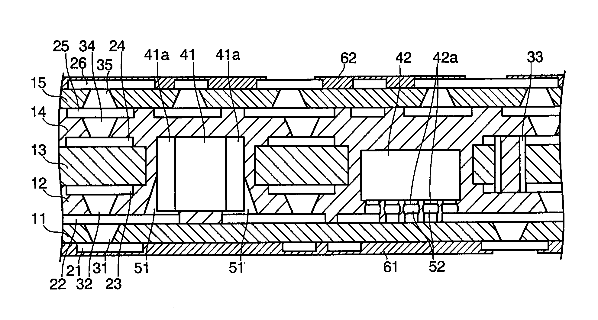
[0054]As a mode of an embodiment according to an aspect of the present invention, the second insulating layer may be a laminated layer of at least two insulating layers, and the component built-in wiring board may further include a second wiring pattern sandwiched between the at least two insulating layers; and an interlayer connector sandwiched between a surface of the wiring pattern and a surface of the second wiring pattern to penetrate partly through the second insulating layer in a layered direction, made of a conductive composition and having a shape with an axis corresponding to the layered direction and a diameter varying in an axial direction. This interlayer connector is an example of an interlayer connector, which is formed in the layered direction to penetrate partly through the second insulating layer in which the electric / electronic component and semiconductor elements are buried, and for example it is an interlayer connector resulting from a conductive bump formed by ...


PUM


Abstract

Disclosed is a component built-in wiring board, including a first insulating layer; a second insulating layer positioned in a laminated state on the first insulating layer; a semiconductor element buried in the second insulating layer, having a semiconductor chip with terminal pads and having surface mounting terminals arrayed in a grid shape connected electrically with the terminal pads; an electric / electronic component further buried in the second insulating layer; a wiring pattern sandwiched between the first insulating layer and the second insulating layer, including a first mounting land for the semiconductor element and a second mounting land for the electric / electronic component; a first connecting member connecting electrically the surface mounting terminal of the semiconductor element with the first mounting land; and a second connecting member connecting electrically the terminals of the electric / electronic component with the second mounting land, made of a same material as a material of the first connecting member.

Description

TECHNICAL FIELD[0001]The present invention relates to a component built-in wiring board having components buried and mounted in an insulating plate, and particularly to a component built-in wiring board having plural kinds of components buried and mounted in mixture. The present invention also relates to a component built-in wiring board having components buried and mounted in an insulating plate, and particularly to a component built-in wiring board having semiconductor chips buried and mounted by flip connection. The present invention also relates to a component built-in wiring board having components buried and mounted in an insulating plate and a manufacturing method thereof, and particularly to a component built-in wiring board in which a component such as a semiconductor chip having terminals arranged at a narrow pitch is buried and mounted and a manufacturing method thereof.BACKGROUND ART[0002]An example of a component built-in wiring board in which plural kinds of components...

Claims


Application Information

Patent Timeline
Patent Type & Authority Applications(United States)
IPC IPC(8): H01L23/498H01L29/66
CPCH01L23/5389H01L24/13H01L2224/32225H01L29/66007H01L23/49861H01L2924/01087H01L2224/131H05K2203/063H05K2203/061H05K2201/10674H05K2201/10636H05K3/4614H05K3/4602H05K3/3442H05K3/3436H05K1/187H05K1/186H01L24/16H01L2224/16225H01L2224/73204H01L2224/81191H01L2224/81192H01L2224/81385H01L2224/81447H01L2224/83192H01L2924/01057H01L2924/01078H01L2924/01079H01L2924/19041H01L2924/00014H01L2924/01014H01L2924/00012H01L2924/00H01L2924/12042H01L2224/05573H01L2224/05568H01L2224/05624H01L2224/05644H01L2224/05647H01L2224/0554H01L2924/19105H01L2224/05548H01L2224/94H01L2224/16238H01L24/05H01L2224/06131Y02P70/50H01L2224/05599H01L2224/0555H01L2224/0556H01L2224/03H01L23/12H01L25/00H05K1/185H05K3/4626H05K3/4691H05K3/46
Inventor SASAOKA, KENJI
Owner DAI NIPPON PRINTING CO LTD
Why Eureka
Try Eureka