
Semiconductor device having impedance calibration function to data output buffer and semiconductor module having the same

a technology of semiconductor modules and semiconductor devices, which is applied in the direction of logic circuit coupling/interface arrangements, pulse techniques, instruments, etc., can solve the problem of difficulty in performing precise calibration operations at all times

Active Publication Date: 2013-04-11
LONGITUDE LICENSING LTD
View PDF6 Cites 42 Cited by
  • Summary
  • Abstract
  • Description
  • Claims
  • Application Information

AI Technical Summary

Benefits of technology

The present patent relates to a semiconductor device and module including a data terminal, calibration terminal, and a plurality of transistor units. The transistor units can be controlled to adjust their impedance, so that the impedance of each unit matches with the impedance of an external resistance. The impedance control circuit uses the electrical potential of the calibration terminal as a reference potential, and reflects the impedance of one of the transistor units to the first transistor unit. This allows for precise control of the impedance of the transistor units, and ensures that the calibration terminal is at the desired potential. The patent also describes a module board on which the semiconductor device is mounted.

Problems solved by technology

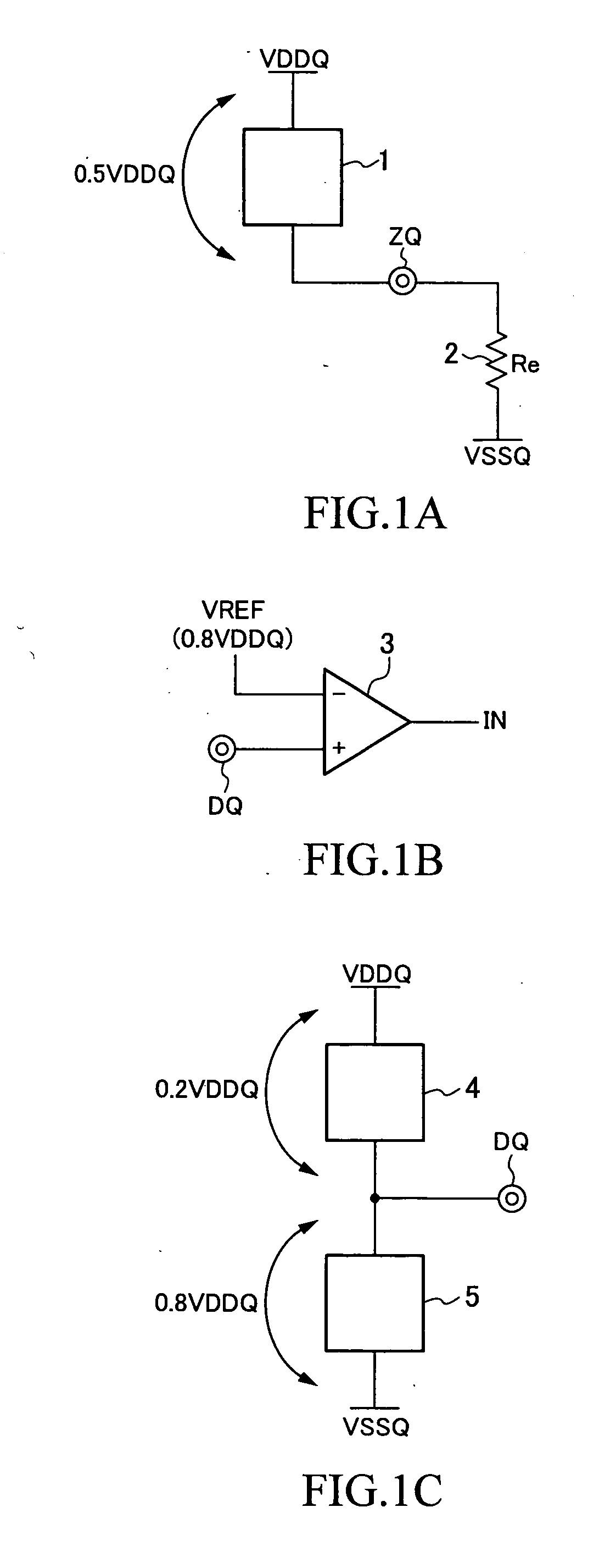
Depending on specifications, however, the reference potential maybe set to the level offset from one half of the power supply potential, which makes it difficult to perform precise calibration operation at all times.

Method used


Image

  • Semiconductor device having impedance calibration function to data output buffer and semiconductor module having the same
  • Semiconductor device having impedance calibration function to data output buffer and semiconductor module having the same
  • Semiconductor device having impedance calibration function to data output buffer and semiconductor module having the same

Examples


second embodiment

[0084]Turning to FIG. 12, the calibration circuit 100a of the second embodiment is a circuit suitable for the case where the level of the reference potential VREF that is used in the input / output circuit 16 is 0.2 VDDQ.

[0085]The calibration circuit 100a shown in FIG. 12 includes four n-type transistor units 161 to 164 that are connected in parallel to the calibration terminal ZQ, four n-type transistor units 171 to 174 that are connected in parallel to the internal node A and one p-type transistor unit 181. The other end of the external resistance 2 that is connected to the calibration terminal ZQ is connected to the power supply potential VDDQ.

[0086]The n-type transistor units 161 to 164 and 171 to 174 are replica buffers of the n-type transistor units 301 to 30n that serve as the pull-down buffers, respectively. Meanwhile, the p-type transistor unit 181 is a replica buffer of each of the p-type transistor units 201 to 20n that serve as the pull-up buffers.

[0087]The potential of th...

third embodiment

[0093]Thus, the plurality of transistor units to be connected to the calibration terminal ZQ can be connected in series.

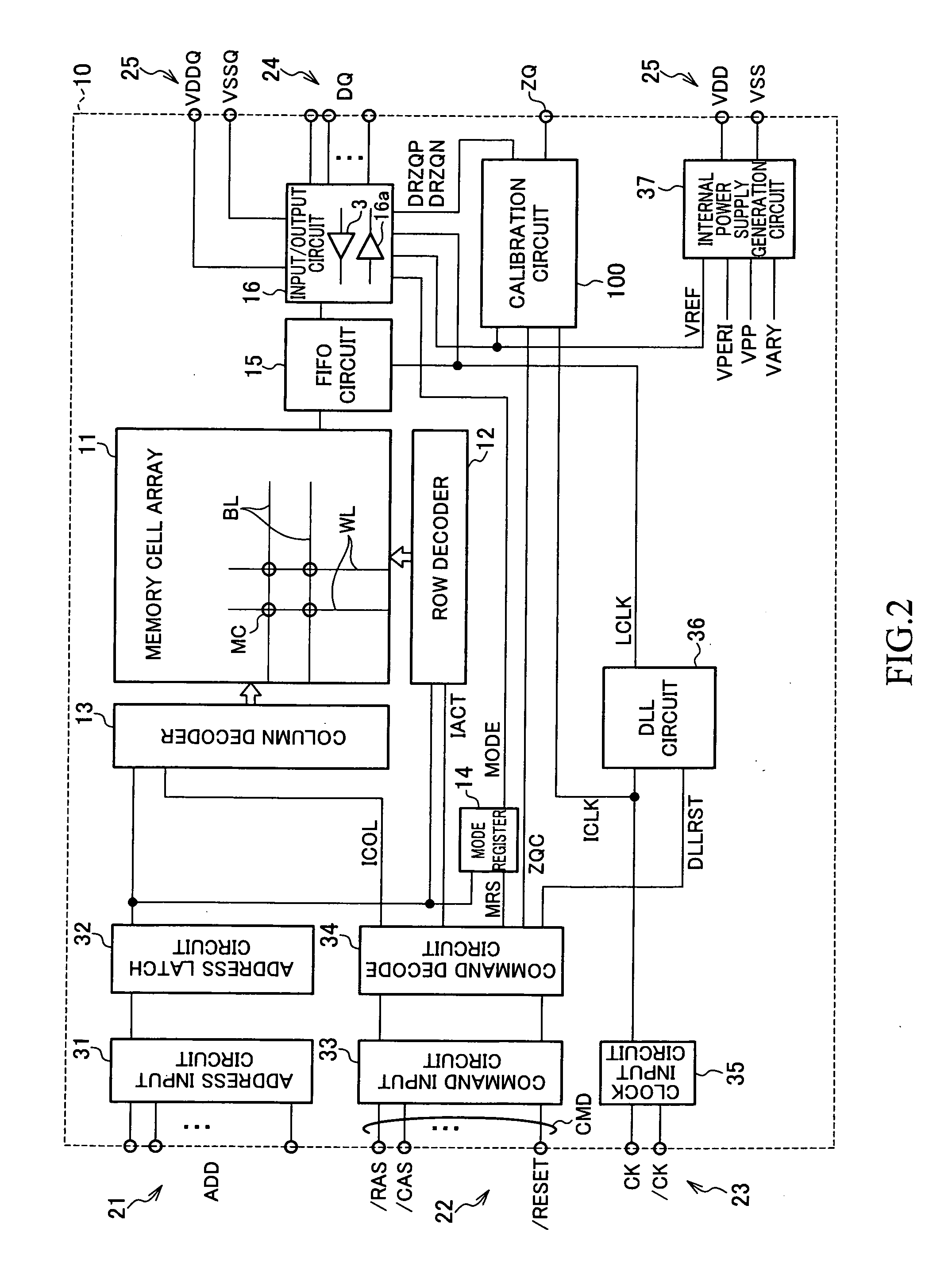
[0094]Turning to FIG. 15, in the information processing system, a data input / output terminal 400 of a controller CNT is commonly connected to data input / output terminals 401 and 402 of memory chips CHIP1 and CHIP2. In the case where a plurality of the data input / output terminals 400 are provided, the data input / output terminals 400 may be individually connected to data input / output terminals 401 and 402, respectively. The memory chips CHIP1 and CHIP2 are devices corresponding to the semiconductor device 10 shown in FIG. 2, and the controller CNT is a device to control the memory chips CHIP1 and CHIP2. According to this embodiment, a calibration terminal ZQ is provided not only in the memory chips CHIP1 and CHIP2, but also in the controller CNT, so as to perform the above-described calibration operation.

[0095]Turning to FIG. 16, the controller CNT includes a contro...


PUM


Abstract

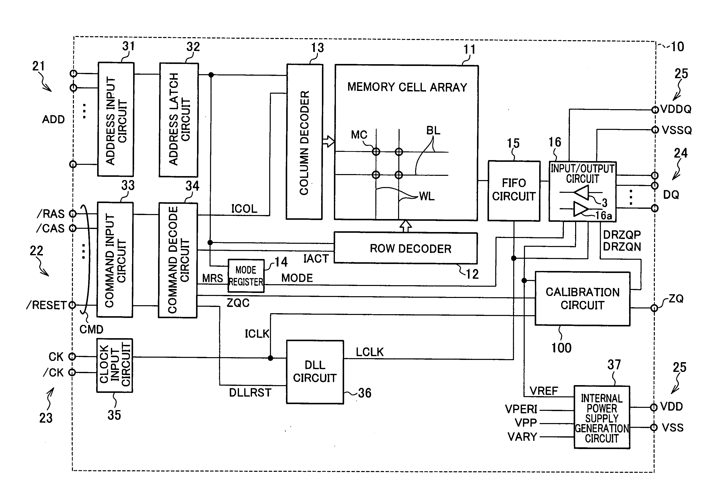
Disclosed herein is a semiconductor device that includes a first transistor unit coupled to the data terminal, and a plurality of second transistor units coupled to the calibration terminal. The first transistor unit includes a plurality of first transistors having a first conductivity type connected in parallel to each other so that an impedance of the first transistor unit is adjustable. Each of the second transistor units includes a plurality of second transistors having the first conductivity type connected in parallel to each other so that an impedance of each of the second transistor units is adjustable. The semiconductor device further includes an impedance control circuit that reflects the impedance of each of the second transistor units to the first transistor unit.

Description

BACKGROUND OF THE INVENTION[0001]1. Field of the Invention[0002]The present invention relates to a semiconductor device and a semiconductor module having the semiconductor device and, in particular, relates to a semiconductor device having an impedance calibration function to a data output buffer and a semiconductor module having the semiconductor device.[0003]2. Description of Related Art[0004]Some semiconductor devices that perform high-speed data transfer, such as DRAM (Dynamic Random Access Memory), include a calibration circuit for adjusting an impedance of a data output buffer. The calibration circuit includes a calibration terminal and a replica buffer connected thereto. The replica buffer is a circuit having substantially the same circuit structure as that of the data output buffer. To the calibration terminal, an external resistance having a target impedance of the data output buffer is connected. Calibration is performed by adjusting impedance of the replica buffer so as t...

Claims


Application Information

Patent Timeline
IPC IPC(8): H03K19/003
CPCH03K19/00315H03K19/094G11C11/4076G11C11/4093G11C2207/2254G11C11/40G11C29/022G11C29/028G11C29/1201G11C29/48H03K19/017545H03K19/0005H01L2924/0002H01L2924/00H03K19/018557G11C11/4094
Inventor HARA, KENTARO
Owner LONGITUDE LICENSING LTD
Learn More