Printed circuit board, antenna, wireless communication device and manufacturing methods thereof

a printed circuit board and antenna technology, applied in the direction of resonant antennas, resistive material coatings, nuclear engineering, etc., can solve the problems of high cost, low supportability for design changes, high cost, etc., to reduce the influence of external objects, low cost, and wide-band characteristics low

Inactive Publication Date: 2013-04-11
FURUKAWA ELECTRIC CO LTD
View PDF4 Cites 28 Cited by
  • Summary
  • Abstract
  • Description
  • Claims
  • Application Information

AI Technical Summary

Benefits of technology

[0080]According to the present invention, a low-loss printed circuit board, a low-loss wide-band antenna, and manufacturing methods thereof can be provided by using a resin as a board material.
[0081]Moreover, according to the present invention, an antenna device having low dielectric loss and reduced influence from external objects and manufacturing methods thereof can be provided.
[0082]Moreover, according

Problems solved by technology

In the two-color molding method, the degree of freedom in the shape of a circuit board and the degree of freedom of the wiring of a conductor pattern are high; however, two molds are required, and cost is high.
Moreover, in order to support design change, the mold

Method used


Image

  • Printed circuit board, antenna, wireless communication device and manufacturing methods thereof
  • Printed circuit board, antenna, wireless communication device and manufacturing methods thereof
  • Printed circuit board, antenna, wireless communication device and manufacturing methods thereof

Examples


fourth embodiment

[0145]The antenna and the manufacturing method thereof, which are the fourth embodiment of the present invention, will be explained below by using FIGS. 5A-5C. In the present embodiment, the antenna 400 equipped with a chip antenna is prepared. FIGS. 5A-5C show processing-step views explaining the manufacturing method of the antenna 400 of the fourth embodiment and is explaining the steps by using top views (left side in the drawing) and lateral views (right side in the drawing).

[0146]FIG. 5A shows a foamed resin material 402 having an interior, in which a foamed part 412 having a foamed structure is formed, and having a surface all of which is covered with a skin layer 411. The foamed resin material 402 has been prepared by molding into a molded body having a predetermined shape in a molding step similar to that of the first embodiment and subjecting this to a foaming step to foam the entire interior thereof. Alternatively, the foamed resin material 402 may be prepared by using pel...

fifth embodiment

[0149]The antenna, the printed circuit board for the antenna, and the manufacturing method thereof, which are the fifth embodiment of the present invention will be explained below by using FIGS. 6A-6D, 7A and 7B. FIGS. 6A-6D show schematic configuration drawings of the antenna and the printed circuit board for the antenna of the fifth embodiment; wherein, FIG. 6A show a top view, FIG. 6B shows a lateral view, FIG. 6C shows a bottom view, and FIG. 6D shows an enlarged lateral view of a cable holder part provided on the printed circuit board for the antenna of the present embodiment. FIGS. 7A and 7B show schematic configuration drawings of the printed circuit board for the antenna of the present embodiment, which is configured so that the board can be equipped with a chip antenna; wherein FIG. 7A shows a top view, and FIG. 7B shows a bottom view.

[0150]The antenna 500 of the present embodiment shown in FIGS. 6A-6D forms an antenna pattern 511 on the upper surface of the printed circuit...

sixth embodiment

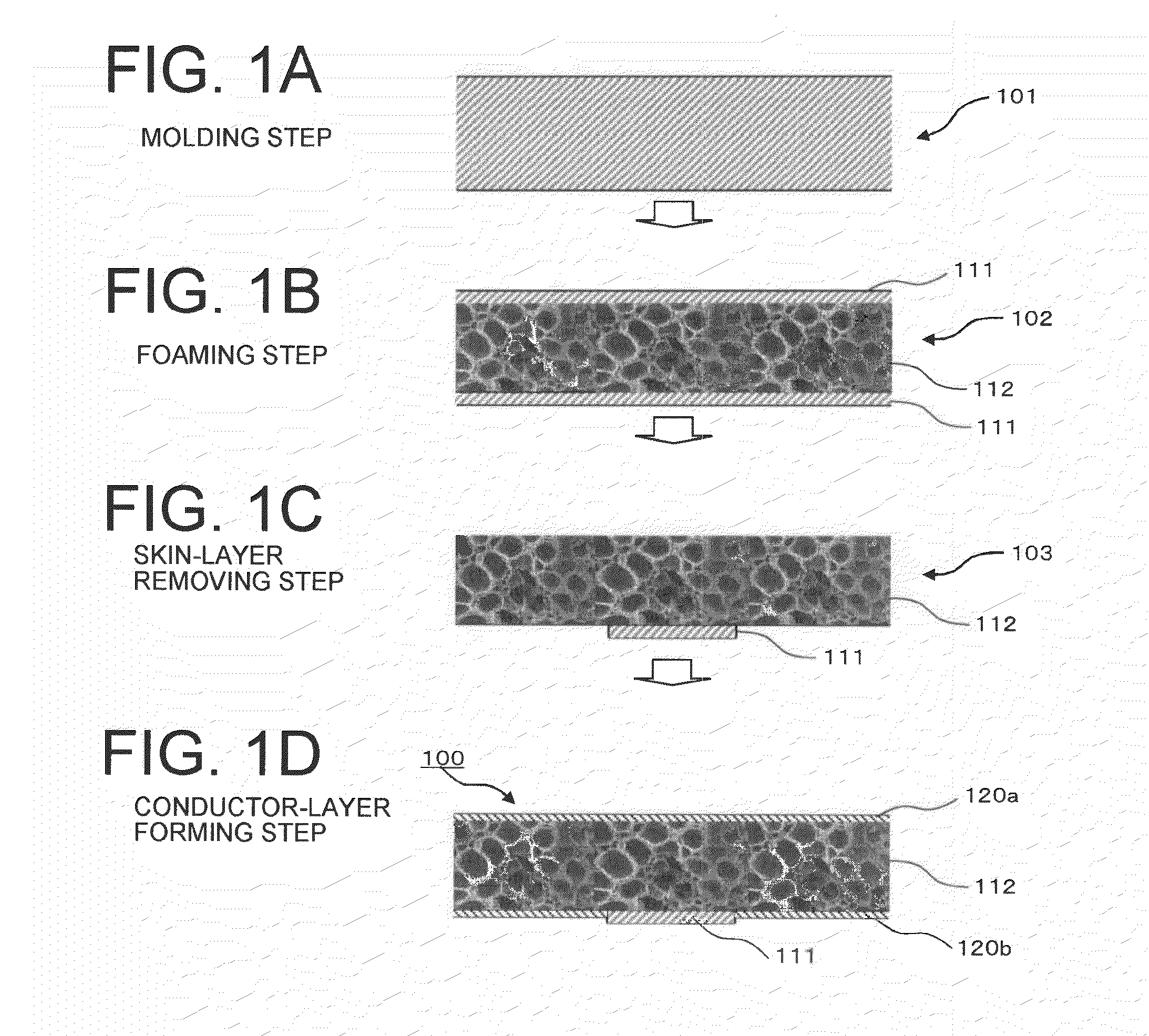
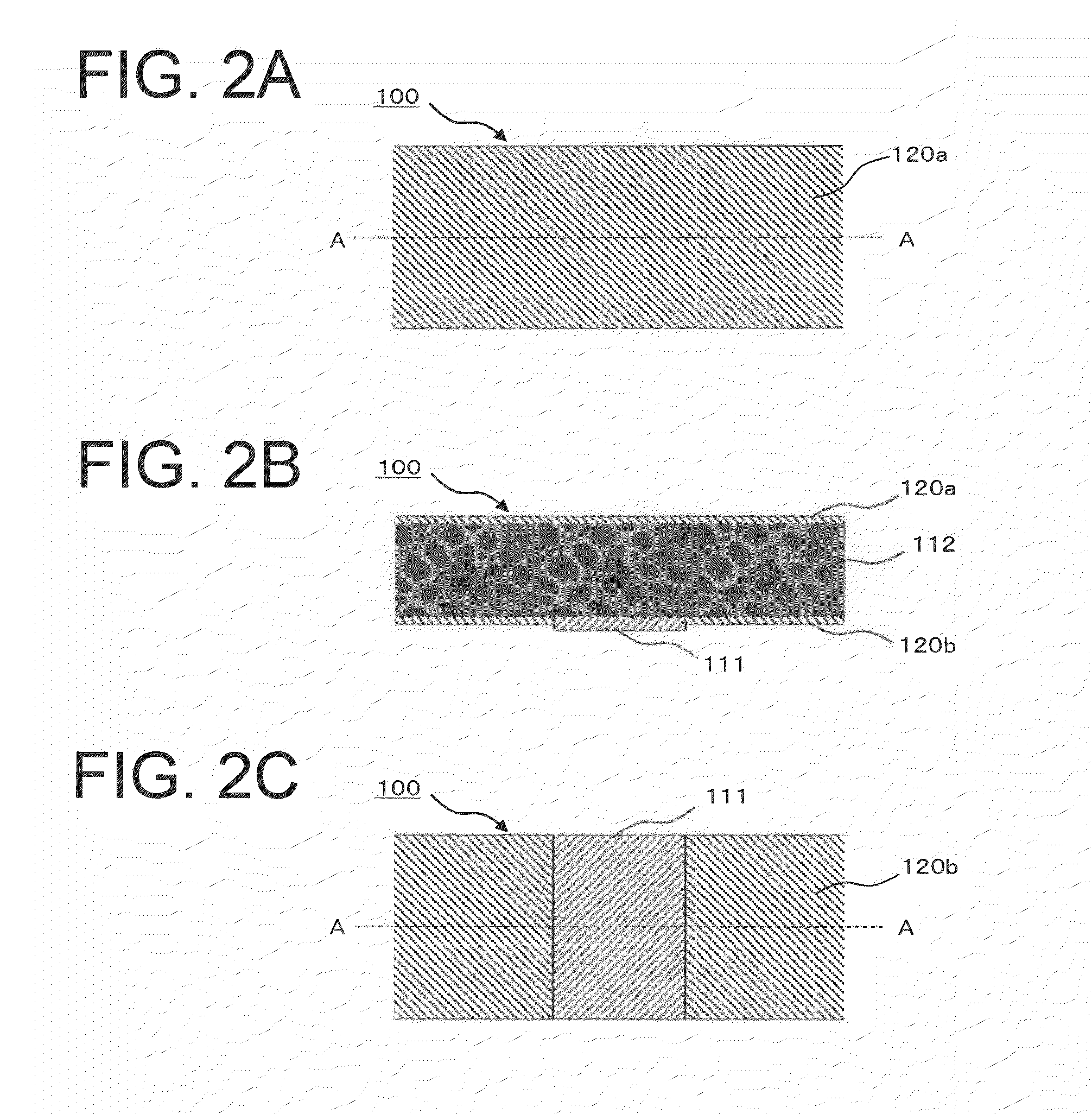
[0155]The printed circuit board and the manufacturing method thereof, which are the six embodiment of the present invention, will be explained below by using FIGS. 8A-8D. FIGS. 8A-8D show processing-step views explaining the manufacturing method of the printed circuit board 600 of the sixth embodiment of the present invention. The present embodiment employs a structure in which a foamed part 612 having a foamed structure is utilized only as an anchor of plating. More specifically, only the region in which the conductor layer 620 is formed by plating is foamed so as to prepare the foamed part 612.

[0156]FIG. 8A shows a resin material 601 prepared by a molding step. PPS or PC (polycarbonate resin) is preferred to be used as the resin that forms the resin material 601. In a foaming step shown in next FIG. 8B, a foamed resin material 602 is prepared by foaming only the upper surface side of the resin material 601 on which the conductor layer 620 is to be formed. It is preferred that the ...


PUM

PropertyMeasurementUnit
Thicknessaaaaaaaaaa
Thicknessaaaaaaaaaa
Angleaaaaaaaaaa

Abstract

Low-loss printed circuit boards, low-loss wide-band antennas, and manufacturing methods thereof are provided by using a resin as a board material. A resin material (101) having a predetermined shape is prepared in a molding step, and the resin material (101) is foamed in a foaming step. As a result, a skin layer (111) and a foamed part (112) are formed. Since the skin layer (111) does not allow close contact of plating, the skin layer (111) is removed in the shape of a conductor pattern in a skin-layer removing step to expose the foamed part (112) in the interior. Electroless plating is carried out in a conductor-layer forming step; and, as a result, plating is brought into close contact with the foamed part (112) having an anchor effect, and a conductor layer (120) is formed.

Description

TECHNICAL FIELD[0001]The present invention relates to printed circuit boards, antennas, wireless communication devices, and manufacturing methods thereof using a resin as a board material and particularly relates to printed circuit boards, antennas, and wireless communication devices formed to have low-dielectric constants by causing the interior of the resin to have a foamed structure and to manufacturing methods thereof.BACKGROUND ART[0002]As manufacturing methods of printed circuit boards using a resin as a board and forming a conductor pattern thereon, a two-color molding method and an insert molding method have been conventionally known. In the two-color molding method, for example, as described in Patent Literature 1, a shape corresponding to a conductor pattern is injection-molded with a first resin to which metal easily adheres, and a shape of a part other than a circuit pattern of the first resin is injection-molded with a second resin to which metal does not easily adhere....

Claims


Application Information

Patent Timeline
IPC IPC(8): H01Q1/38H01Q1/50H01Q21/00H05K1/03
CPCH01Q1/36H01Q1/38H01Q9/42H05K1/0393H05K1/03H05K3/185H05K2201/09118H01Q1/50H01Q21/00H05K3/146H05K2201/0116H05K2201/10098
Inventor HAMADA, HIROKITAMAOKA, HIROYUKIISO, YOICHI
Owner FURUKAWA ELECTRIC CO LTD
Why Eureka
Try Eureka