OLED Display Driver Circuits and Techniques

a technology of organic light-emitting diodes and driver circuits, which is applied in the direction of electrical equipment, instruments, semiconductor devices, etc., can solve the problems of large variability of polysilicon, and achieve the effects of reducing silicon cost, increasing silicon area, and reducing silicon area

Inactive Publication Date: 2013-04-11
CAMBRIDGE DISPLAY TECH LTD
View PDF4 Cites 157 Cited by
  • Summary
  • Abstract
  • Description
  • Claims
  • Application Information

AI Technical Summary

Benefits of technology

[0006]Embodiments of the above described technique; although they employ an additional, cascode transistor enable the use of a lower voltage process, with an overall reduction in the area of silicon, and thus a concomitant reduction in silicon cost.
[0007]In embodiments the chiplets are provided with a power supply connected to the first, for example VDD power supply line / connection of a chiplet, and to the second, for example ground, power supply connection to a chiplet, which may comprise a connection to the substrate of the chiplet. The power supply defines a power supply voltage range and the techniques we describe enable an associated OLED pixel to be driven with a voltage outside this range. For example a drain connection of the cascode transistor may be connected to an anode of the associated OLED pixel and the cathode of the OLED pixel may be connected to an OLED power supply line or connection at a negative voltage, that is below the substrate potential (ground). In this way the voltage swing on the OLED as it is driven between fully off and fully on states may be greater than the power supply voltage range of the chiplet. Furthermore the techniques we describe are able to achieve this without requiring level shifters between the pixel driver control circuitry and output stage, which would otherwise increase the silicon area.

Problems solved by technology

The use of thin film transistors has a number of associated difficulties, in particular because amorphous silicon is unstable in that its threshold voltage and carrier mobility shifts over extended periods of use, whilst polysilicon often exhibits a large degree of variability in the same parameters across the display substrate.

Method used


Image

  • OLED Display Driver Circuits and Techniques
  • OLED Display Driver Circuits and Techniques
  • OLED Display Driver Circuits and Techniques

Examples


Embodiment Construction

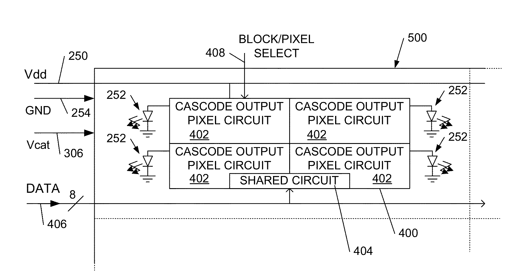
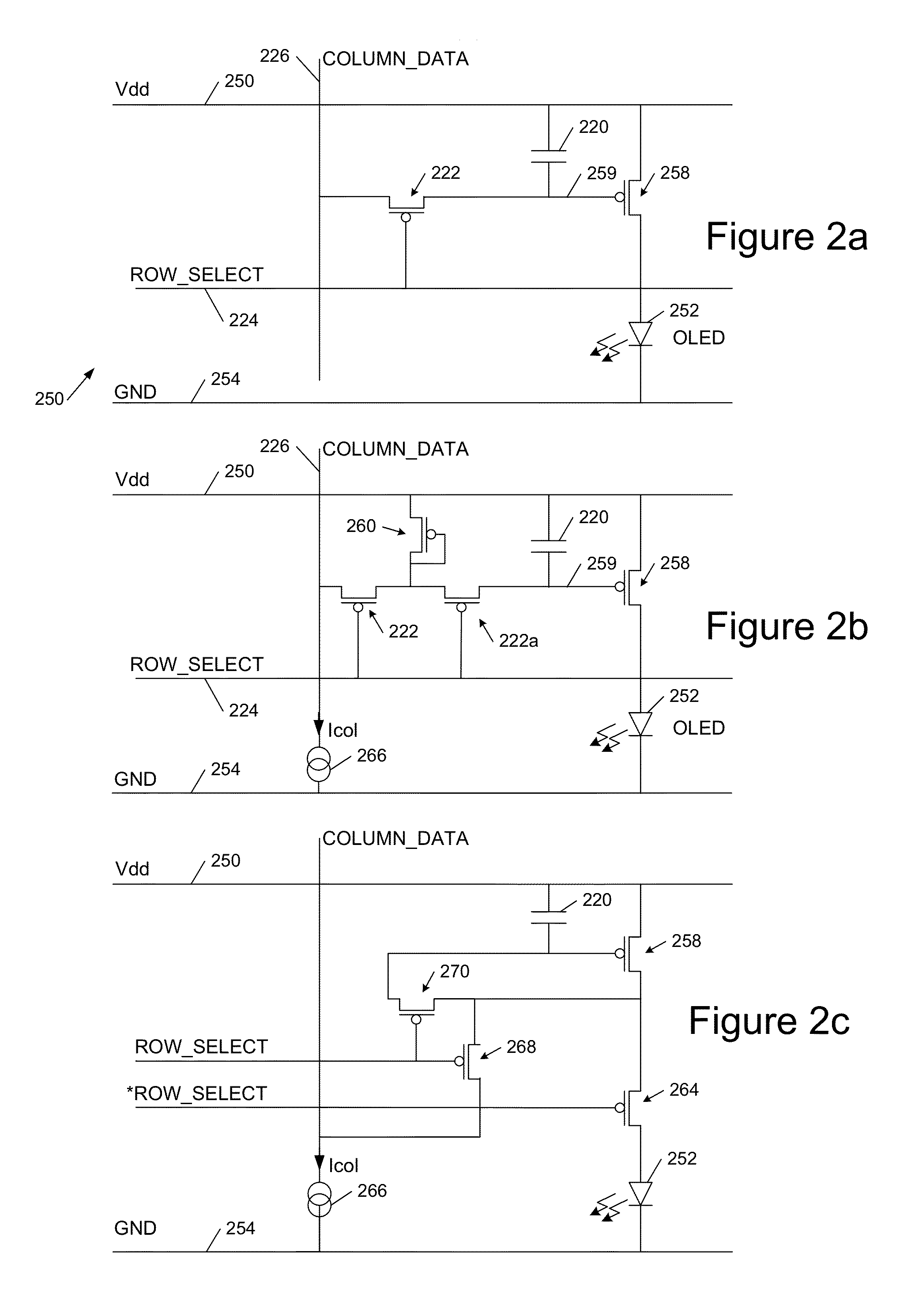
[0020]Broadly speaking we will describe pixel driver circuit techniques for inclusion of an output cascode stage where the output can drop below ground potential. Further, the output can be used at a greater voltage than that of the silicon process, and the techniques enable a higher voltage range output than that of the nominal silicon process.

[0021]We first describe example chiplets and pixel driver circuits, as this is helpful for understanding embodiments of the invention.

Chiplets

[0022]Implementations of the embodiments of the invention use chiplets for the pixel drive circuitry. In broad terms these comprise small silicon integrated circuits which are stuck onto the glass substrate of a display and connected to OLED pixels and to external connections of the display.

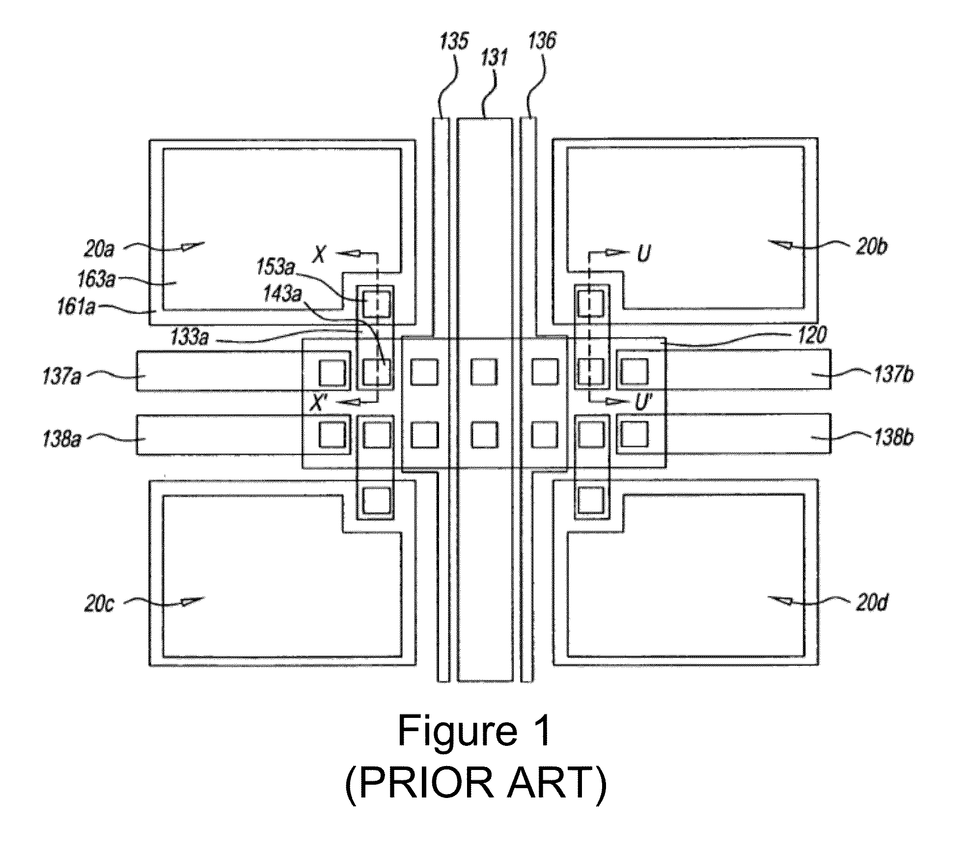
[0023]FIG. 1 which is taken from WO 2010 / 019185 shows a layout view of a group of four pixels (20a, 20b, 20c and 20d) elements of an OLED display device. Each of the four pixels can be arranged to emit a different co...


PUM


Abstract

We describe a method of driving an OLED display. The OLED display comprises a plurality of pixel driver circuits on chiplets, each pixel driver circuit comprising an output transistor for driving a first connection of an associated OLED pixel. A cascode transistor on the chiplet is coupled between the output transistor and the first connection of said associated OLED pixel. A power supply is provided to the chiplet, defining a chiplet voltage range. A second connection of the associated OLED pixel is connected to an OLED voltage outside said chiplet voltage range. The OLED pixel is then driven using the pixel driver circuit on the chiplet over an OLED voltage range greater than said chiplet voltage range. In some preferred embodiments a drain connection of the cascode transistor is set at a voltage below a ground or negative (Vss) power supply to a chiplet.

Description

FIELD OF THE INVENTION[0001]This invention relates to techniques for driving organic light emitting diodes (OLED) displays, in particular using display driver circuitry fabricated on a plurality of small integrated circuits (chiplets).BACKGROUND TO THE INVENTION[0002]It is known to drive an OLED display using an active matrix arrangement in which individual pixels of the display are activated by an associated thin film transistor (TFT). The brightness of an OLED pixel of such a display may be programmed by either a voltage or a current. (In this specification references to ‘pixels’ are to be interpreted as including different coloured sub-pixels of a colour display). In either case a typically memory element is associated with each pixel so that the data written to a pixel is retained whilst other pixels are addressed. Generally this is achieved by a storage capacitor which stores a voltage set on the gate of a driver transistor, which in turn dictates the current through the OLED p...

Claims


Application Information

Patent Timeline
Patent Type & Authority Applications(United States)
IPC IPC(8): G09G3/32
CPCG09G3/3233H01L27/3255G09G2300/0861H10K59/129H10K59/123
Inventor SMITH, EUAN C.RANKOV, ALEKSANDRA
Owner CAMBRIDGE DISPLAY TECH LTD
Why Eureka
Try Eureka