Memory controller and storage device

a memory controller and storage device technology, applied in the field of memory controllers and storage devices, can solve the problems of affecting the performance of flash memory, affecting the operation of flash memory, and forming many electron traps, so as to achieve the effect of reducing the number of read commands, high speed, and achieving reading performan

Active Publication Date: 2013-04-11
PANASONIC CORP
View PDF6 Cites 5 Cited by
  • Summary
  • Abstract
  • Description
  • Claims
  • Application Information

AI Technical Summary

Benefits of technology

[0027]Based on the above configuration, when the first read unit corresponds to two pages of a memory, for example, the number of read commands can be substantially decreased, when addresses of a read command equal to or larger than a predetermined size or a series of read commands are continuous. As a result, reading performance can be achieved at a high speed.
[0028]When the second read unit is 512 bytes (=1 sector), for example, a reading error from each memory is detected in a one-sector unit. The first ECC correcting unit corrects data of an error-detected sector, by using data of a sector in which a reading error is not detected. Because an error can be corrected in a one-sector unit, an effect of error correction can be fully exerted.
[0029]That is, both high-speed reading and securing of reliability can be achieved, by using both a first read process of reading in a relatively large block, and a second read process of reading in a small block by attaching weight to precision of error correction.
[0030]Therefore, in the following embodiments, to solve the above problems, there are proposed a controller and the like that can achieve a stable high-speed read transfer while improving an error resistance by an iterated code configuration.

Problems solved by technology

Further, when data rewriting is repeated each time the number of times of rewriting increases, a slight damage occurs in a gate oxide film by injection and extraction of electrons.
When these damages are accumulated, many electron traps are formed.
In this way, in accordance with the multiple-value recording that supports a larger capacity of the flash memory and miniaturization of a semiconductor process, a problem of degradation in the data holding characteristic of the flash memory has become noticeable.
However, variation in the data holding characteristic of a cell of the flash memory cannot be shielded by the leveling.
A problem when the Management-NAND is used instead of a flash memory in the configuration of Japanese Unexamined Patent Publication No. 2006-18373, for example, is described below.
In the case of reading data from a memory card in which the data is written in this way, there is a following problem.
When a reading error occurs, the reading error is notified by an interruption signal or the like.
Therefore, a processing time at the time of occurrence of an error becomes large.
As a result, at a position where a reading error occurs in video data reproduction, a transfer rate drops extremely, and omission of a video frame and the like occurs.
When a read command is issued in each Management-NAND in a sector unit to avoid the above operation, a process becomes simple, but a command overhead becomes large.

Method used


Image

  • Memory controller and storage device
  • Memory controller and storage device
  • Memory controller and storage device

Examples


first embodiment

0. Configuration Example

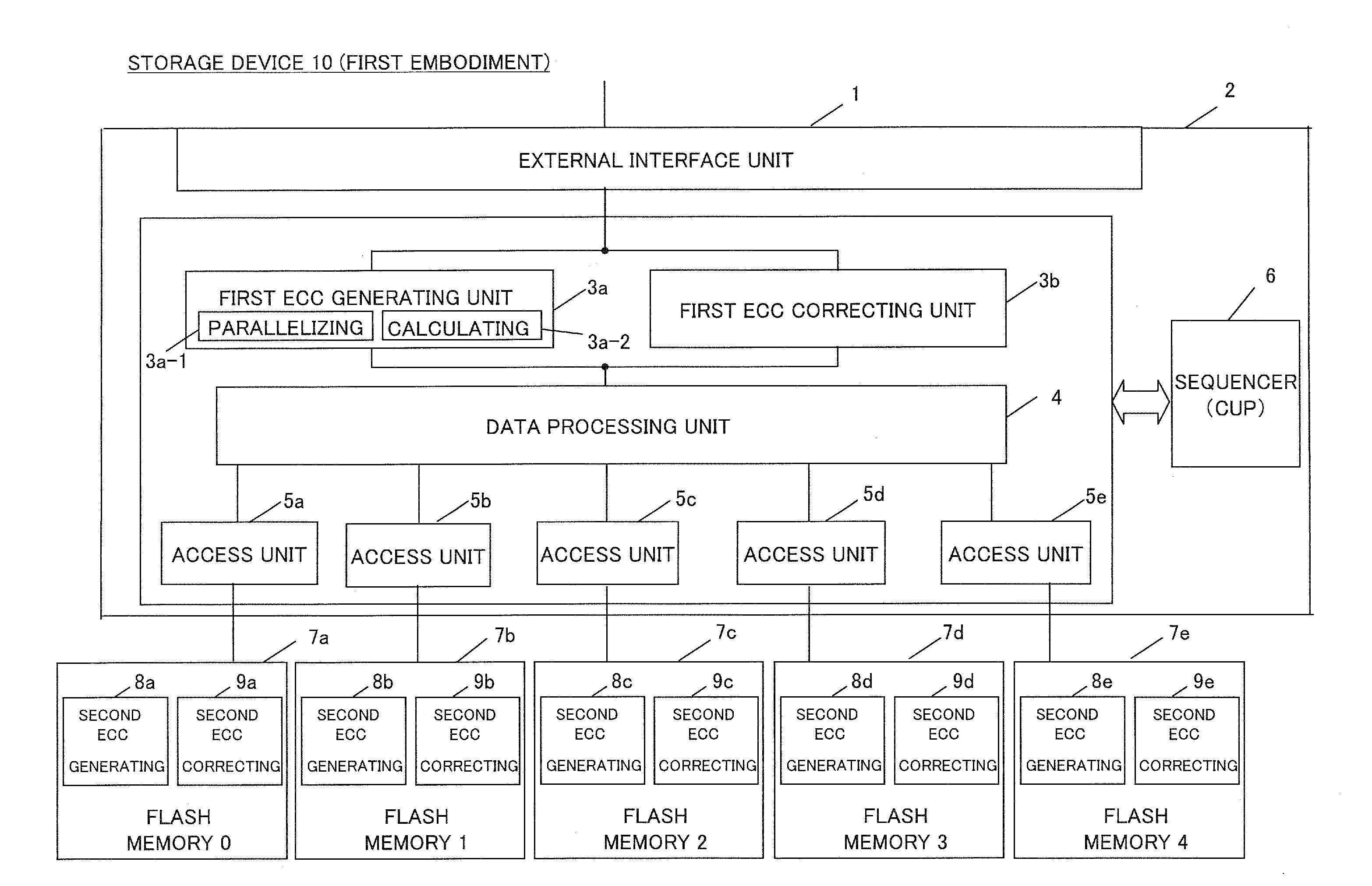
[0040]FIG. 3 is an overall configuration diagram of a storage device 10 according to a first embodiment. The storage device 10 according to the first embodiment includes a plurality of flash memories 7a to 7e, each incorporating therein an error correction processing unit, and a memory controller 2 that writes and reads data to and from the flash memories 7a to 7e.

[0041]FIG. 4 is a configuration diagram of an erase block of the flash memories 7a to 7e used in the first embodiment.

[0042]The flash memories 7a to 7e are configured by a plurality of erase blocks, and each erase block is configured by a plurality of pages. The erase block shown in FIG. 4 is configured by 128 pages including page 0 to page 127, and data writing and reading are performed in a page unit. For example, when a data capacity per one page is 8 KB, an erase block size becomes 1 MB. When the number of erase blocks is 1 K, a capacity of the flash memory becomes 1 GB.

[0043]The flash memories...

second embodiment

Configuration Example

[0104]A configuration according to a second embodiment is substantially similar to that in the first embodiment, and therefore, a detailed description thereof is omitted.

[0105]In the first embodiment, the first ECC code is a (5, 4) ECC code, and this code is applied to only one error correction. On the other hand, in the present embodiment, the first ECC code is a (10, 8) ECC code, and this is applied to correction of double errors.

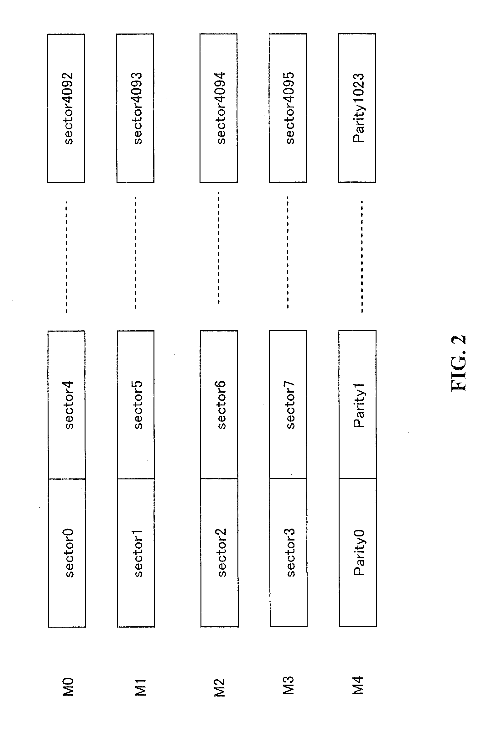
[0106]The first ECC generating unit 3a in the first embodiment allocates continuous 2-Kbyte data to four flash memories in a 512-byte unit, calculates EXOR of 4-byte data obtained by extracting each one byte from the 512-byte data allocated to each flash memory, and generates 1-byte parity data.

[0107]The first ECC generating unit 3a in the present second embodiment allocates continuous 64-Kbyte data to four flash memories 7a to 7d in a 16-Kbyte unit, and extracts each two byte from the 16

[0108]Kbyte-data allocated to each flash memory...


PUM


Abstract

According to one embodiment, a memory controller that writes write data provided from a host device into a memory, reads read data from the memory, and transmits the read data to the host device. The memory controller includes an external interface, a first ECC generating unit, an access unit, a first ECC correcting unit, and a control unit.

Description

BACKGROUND[0001]1. Technical Field[0002]The present disclosure relates to a memory controller and a storage device and the like that control to suppress degradation due to variation in a data holding characteristic and the number of times of rewriting of a nonvolatile memory.[0003]2. Related Art[0004]Conventionally, a semiconductor storage device such as an SD (Secure Digital) card as a card-type recording medium which incorporates therein a flash memory is extremely compact and extremely thin. Because of its easiness of handling, the semiconductor storage device is widely used to record data such as images in digital cameras and portable devices.[0005]The flash memory incorporated in the semiconductor storage device is configured by many physical blocks of a fixed size, and can erase data in a unit of a physical block. To respond to recent demands for a larger capacity, multiple-value flash memories (MLC: Multi-Level Cell) that can accumulate data of two or more bits in one cell ar...

Claims


Application Information

Patent Timeline
Patent Type & Authority Applications(United States)
IPC IPC(8): G06F11/08
CPCH03M13/03H03M13/2957G06F11/1068H04L1/0051H03M13/2975
Inventor OOTSUKA, TAKESHI
Owner PANASONIC CORP
Why Eureka
Try Eureka