

Semiconductor device and method for manufacturing semiconductor device
a semiconductor and semiconductor technology, applied in the direction of semiconductor devices, basic electric elements, electrical equipment, etc., can solve the problems of reducing the yield of transistors in the manufacturing process, affecting the quality of semiconductor devices, so as to reduce the damage to the oxide semiconductor layer or the effect of reducing the film thickness, suppressing the on-state current, and reducing the cos
- Summary
- Abstract
- Description
- Claims
- Application Information
AI Technical Summary
Benefits of technology
Problems solved by technology
Method used
Image

Examples
embodiment 1
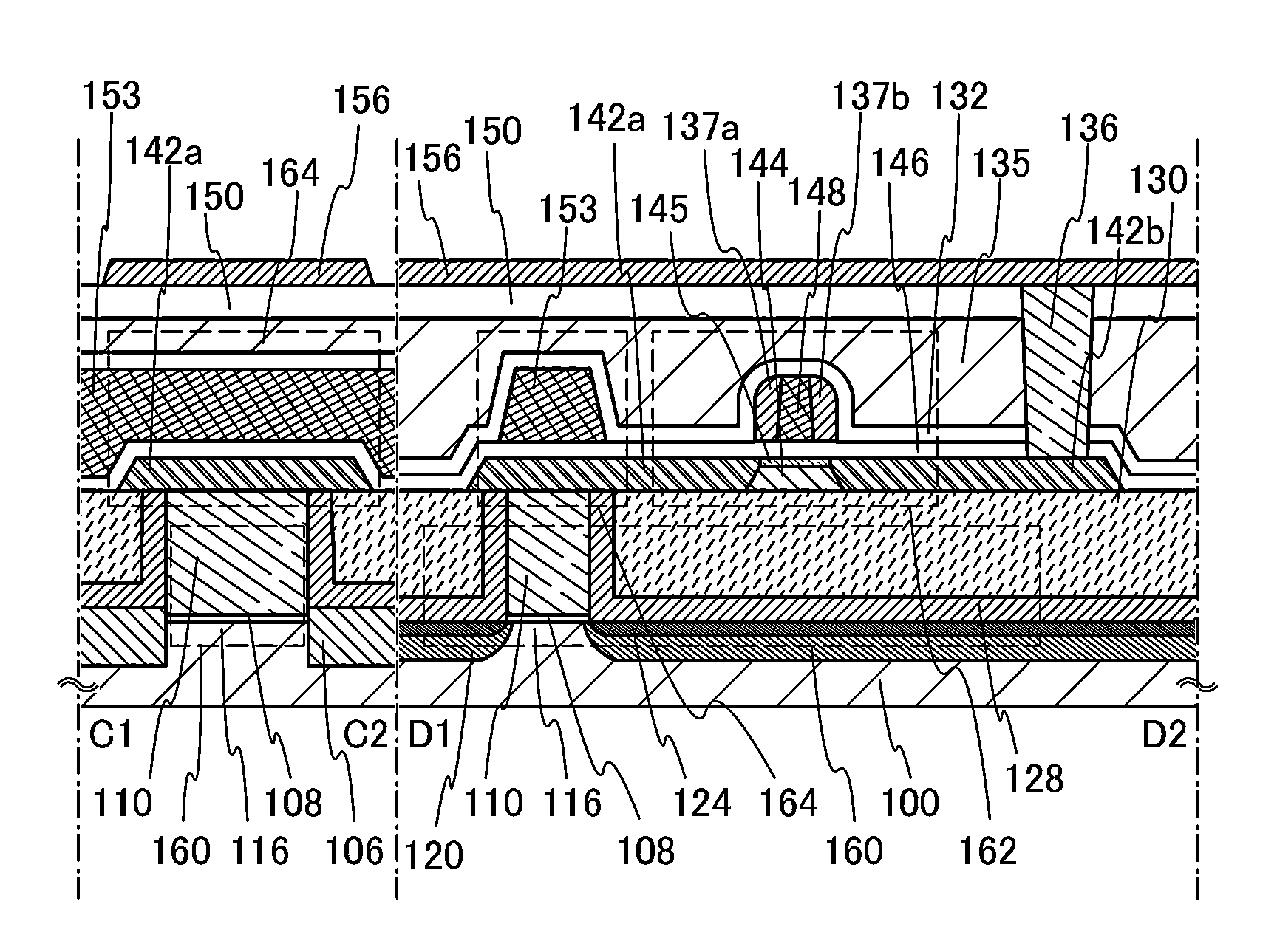
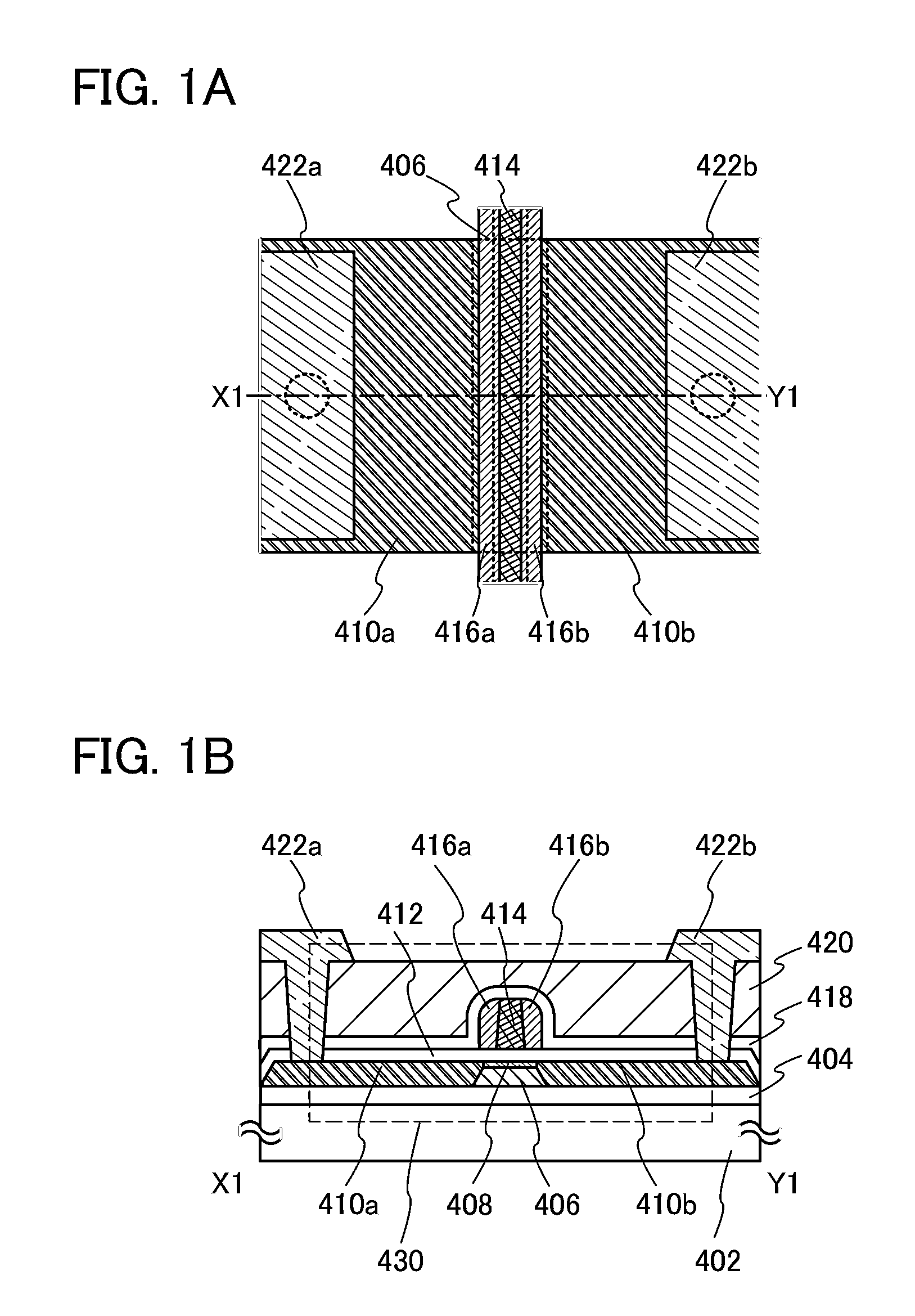
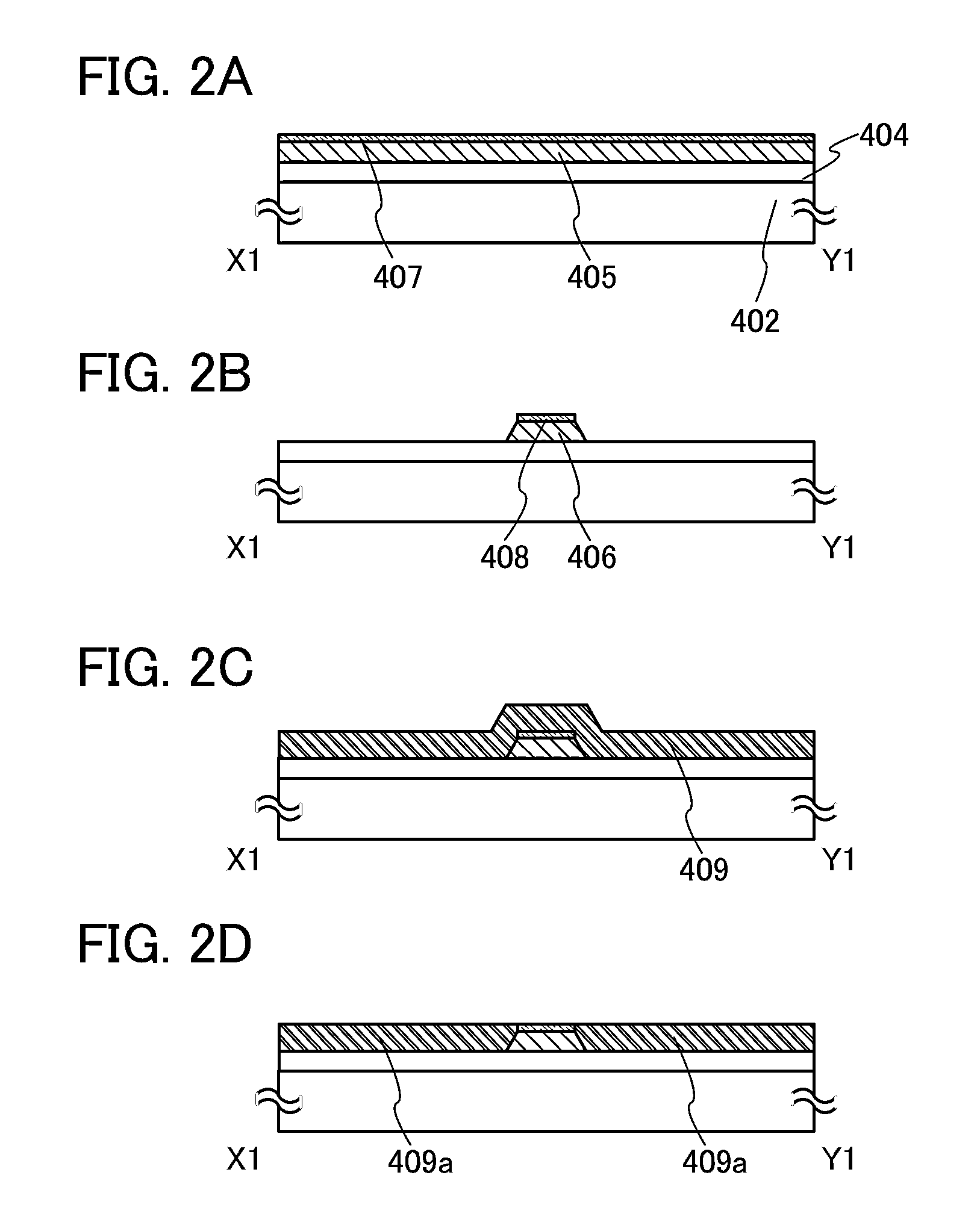
[0053]In this embodiment, one embodiment of a semiconductor device and a method for manufacturing the semiconductor device will be described with reference to FIGS. 1A and 1B, FIGS. 2A to 2D, and FIGS. 3A to 3D.
[0054]FIGS. 1A and 1B are a plan view and a cross-sectional view illustrating a transistor 430 as an example of a semiconductor device. FIG. 1A is a plan view of the transistor 430, and FIG. 1B is a cross-sectional view taken along the line X1-Y1 in FIG. 1A. Note that in FIG. 1A, some components of the transistor 430 (e.g., an insulating layer 420) are not illustrated for simplicity.
[0055]The transistor 430 illustrated in FIGS. 1A and 1B includes, over a substrate 402, a base insulating layer 404; a source electrode layer 410a; a drain electrode layer 410b; an oxide semiconductor layer 406 of which one side surface is in contact with the source electrode layer 410a and the other side surface is in contact with the drain electrode layer 410b in the cross section in the channel...
embodiment 2
[0158]In this embodiment, modification examples of the semiconductor device and the method for manufacturing the semiconductor device described in Embodiment 1, which are illustrated in FIGS. 1A and 1B, FIGS. 2A to 2D, and FIGS. 3A to 3D, will be described with reference to FIGS. 4A and 4B, FIGS. 5A to 5D, and FIGS. 6A to 6D. Note that portions similar to those in FIGS. 1A and 1B, FIGS. 2A to 2D, and FIGS. 3A to 3D are denoted by the same reference numerals, and description thereof is repeated.
[0159]FIGS. 4A and 4B are a plan view and a cross-sectional view illustrating the transistor 440 as an example of a semiconductor device. FIG. 4A is a plan view of the transistor 440, and FIG. 4B is a cross-sectional view taken along the line X2-Y2 in FIG. 4A. Note that in FIG. 4A, some components of the transistor 440 (e.g., the insulating layer 420) are not illustrated for simplicity.
[0160]The transistor 440 illustrated in FIGS. 4A and 4B includes, over the substrate 402, the base insulating...
embodiment 3
[0208]In this embodiment, a modification example of the semiconductor device which is described in Embodiment 1 and illustrated in FIGS. 1A and 1B, and a modification example of the semiconductor device which is described in Embodiment 2 and illustrated in FIGS. 4A and 4B will be described with reference to FIGS. 7A and 7B and FIGS. 8A and 8B. Note that portions similar to those in FIGS. 1A and 1B and FIGS. 4A and 4B are denoted by the same reference numerals, and description thereof is not repeated.
[0209]FIGS. 7A and 7B are a plan view and a cross-sectional view illustrating the transistor 450 as an example of a semiconductor device. FIG. 7A is a plan view of the transistor 450, and FIG. 7B is a cross-sectional view taken along the line X3-Y3 in FIG. 7A. Note that in FIG. 7A, some components of the transistor 450 (e.g., the insulating layer 420) are not illustrated for simplicity.
[0210]The transistor 450 illustrated in FIGS. 7A and 7B includes, over the substrate 402, the base insu...
PUM
 Abstract
Description
Claims
Application Information