Light emitting device

a technology of light emitting device and light emitting element, which is applied in the direction of semiconductor devices for light sources, point-like light sources, lighting and heating apparatus, etc., can solve the problems of not economically viable, changing the color temperature of the emission color of the light emitting device which uses a semiconductor light emitting element is relatively expensive in comparison with a fluorescent lamp, so as to achieve the effect of simple color temperature adjustment, simple emission spectrum adjustment, and superior emission efficiency

Inactive Publication Date: 2013-04-18
MITSUBISHI CHEM CORP
View PDF23 Cites 150 Cited by
  • Summary
  • Abstract
  • Description
  • Claims
  • Application Information

AI Technical Summary

Benefits of technology

[0054]The present invention makes it possible to provide a light emitting device of a superior emission efficiency which enables straightforward adjustment of an emission spectrum. Furth...

Problems solved by technology

A light emitting device which uses a semiconductor light emitting element is relatively costly in comparison with a fluorescent lamp, and changing the color temperature of the emission color of a light emitting device according to the environment or season, just as a fluorescent lamp is replaced in summer and winter, is not economically viable.
However, such a light emitting device has low light rendering properties, forming white light from the blue light which is emitted by the light emitting element and yellow light which is emitted by the phosphor through excitation with the light which is emitted from the light emitting element.
However, there is a problem in that, in the light emitting device according to Japanese Patent Application Publication No. 2009-245712, in a case where a plurality of phosphor of different emission colors is contained mixed in the phosphor layer in order to raise the color rendering properties, a phenomenon arises whereby phosphor of another type absorbs the fluorescent light emitted by a certain type of phosphor, that is, cascade excitation arises, and the light emission efficiency of the phosphor layer is low (first problem).
Further, in the light emitting device according to Japanese Patent Application Publication No. 2009-245712, the way in which the distance between the phosphor layer and the semiconductor light emitting device is configured is not defined, and when there is an inadequate separation distance between the phosphor layer and the semiconductor light emitting element, an...

Method used


Image

  • Light emitting device
  • Light emitting device
  • Light emitting device

Examples


second embodiment

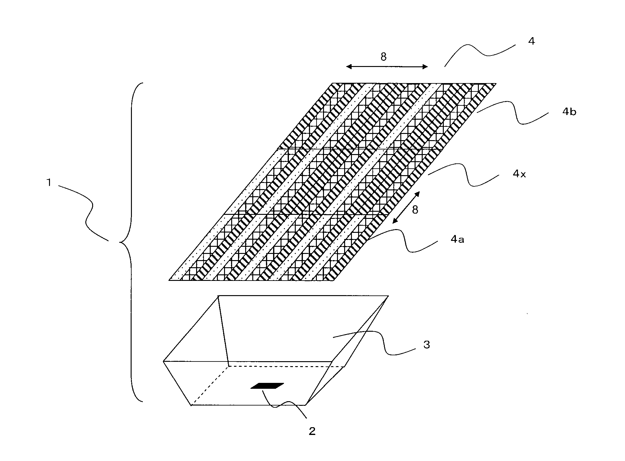
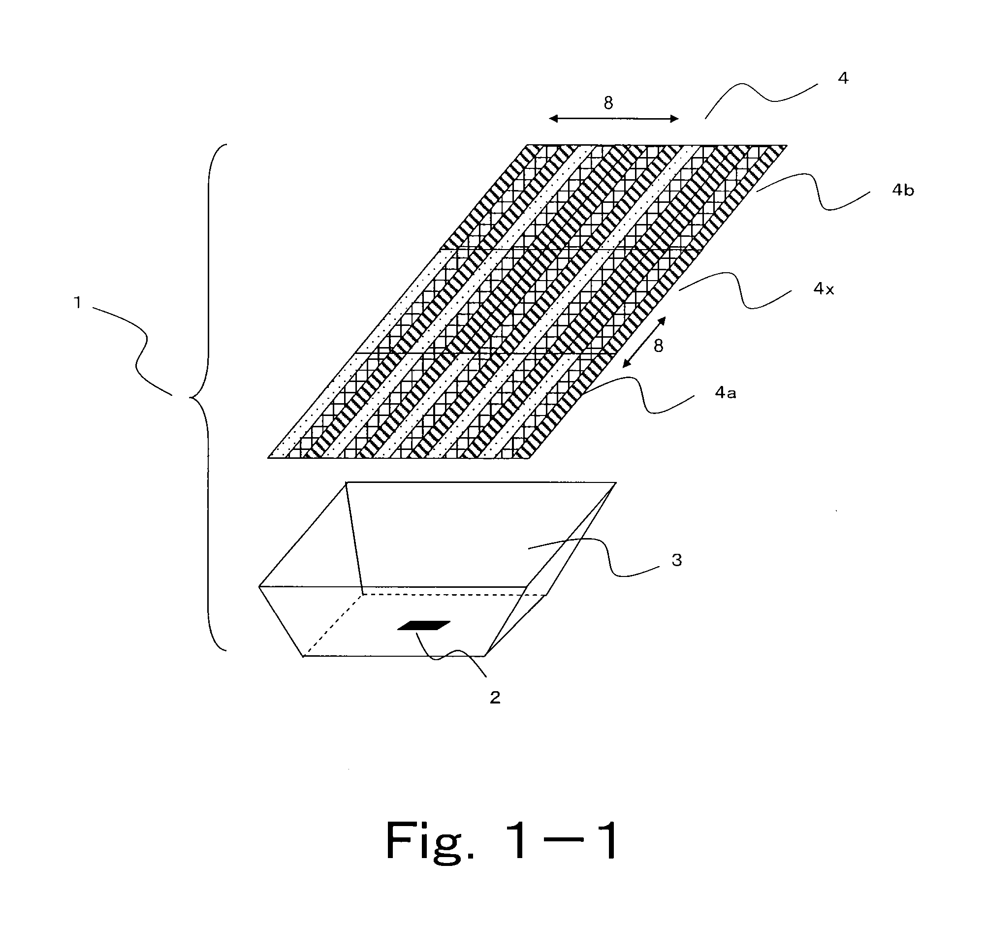
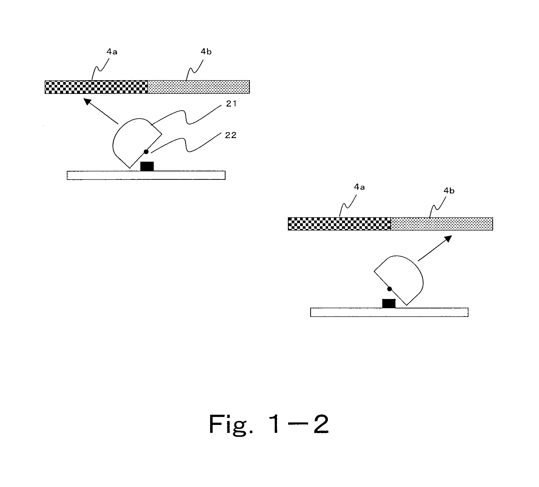
[0305]A second embodiment will be described next. FIG. 23 serves to schematically show an axis orthogonal cross section of a light emitting device 11 according to a second embodiment. Here, the focus of the description will be on points of difference from the configuration of the first embodiment (the cross sectional structure shown in FIG. 17 in particular) and points in common will not be described here. In this embodiment, the housing member 14 comprises a phosphor layer 141 formed on the inner peripheral side of the transparent base material. Meanwhile, a bandpass filter (so-called ultraviolet cut filter) 15 which reflects the light (excitation light) emitted by the light emitting diode 12 and transmits the light emitted by each of the phosphors contained in the phosphor layer 141 is provided on the outer peripheral side of the transparent base material. A commercially available bandpass filter can be suitably used as the bandpass filter 15, and the type of the bandpass filter 1...

third embodiment

[0310]A third embodiment will be described next. FIGS. 25A and 25B serves to schematically show an axis orthogonal cross section of the light emitting device 11 according to the third embodiment. Here, the focus of the description will be the characteristics of this embodiment. In this embodiment, the light emitting diode 12 is disposed on both faces of the substrate 13 such that the substrate 13 is held from both sides. Here, the light emitting diode 12 mounted on the lower face of the substrate 13 is called the “first light emitting diode 12a” and the light emitting diode 12 mounted on the upper face is called the “second light emitting diode 12b”.

[0311]As is illustrated, the first light emitting diode 12a and the second light emitting diode 12b are disposed at the back with the substrate 13 held from both sides. Hence, the irradiation center direction Dc of the first light emitting diode 12a is oriented vertically downward with reference to the substrate 13 and the irradiation c...

fourth embodiment

[0314]A fourth embodiment will be described next. FIG. 26 schematically shows an axis orthogonal face of the light emitting device 11 according to a fourth embodiment. Here, the description will focus on the characteristics of this embodiment. Similarly to the first embodiment and so on, the light emitting device 11 according to this embodiment has a light emitting diode 12 mounted only on the lower face of the substrate 13. Here, in the space where the housing member 14 is housed, the space opposite the upper face of the substrate 13 is called the “power source back side space.”

[0315]A heat radiation fin 18 for radiating the heat of the light emitting diode 12 is disposed in thermal contact with the upper face of the substrate 13 in the foregoing light source back side space SNL. The material values of the substrate 13 such as thermal conductivity are adjusted so that the heat emitted by the light emitting diode 12 is efficiently conducted to the heat radiation fin 18. Note that ea...


PUM


Abstract

An object of the present invention is to provide a light emitting device exhibiting a superior emission efficiency which enables easy adjustment of an emission spectrum.
The above object is achieved by a light emitting device comprising a semiconductor light emitting element and a phosphor layer, which has an area A and an area B of different emission spectra, and in which a plurality of phosphor portions are disposed on a plane such that identical phosphor portions do not adjoin one another, and the surface area occupied by specific phosphor portions in the phosphor layer is different in area A and area B.

Description

TECHNICAL FIELD[0001]The present invention relates to a light emitting device and, more particularly, to a light emitting device exhibiting a superior emission efficiency which enables easy adjustment of an emission spectrum.BACKGROUND ART[0002]A light emitting device which uses a semiconductor light emitting element is relatively costly in comparison with a fluorescent lamp, and changing the color temperature of the emission color of a light emitting device according to the environment or season, just as a fluorescent lamp is replaced in summer and winter, is not economically viable. It is desirable to be able to change the color temperature, where necessary, of a single light emitting device.[0003]In order to meet this requirement, Japanese Patent Application Publication No. 2009-245712 discloses a light emitting device in which phosphor of different emission colors is applied to a central portion and outer periphery of a transparent disk, in which the irradiation angle is changed...

Claims


Application Information

Patent Timeline
IPC IPC(8): H01L33/50F21V9/40
CPCF21K9/56F21V29/83F21Y2101/02F21Y2103/003H01L25/0753H01L33/504H01L33/505H01L33/507H01L33/508F21V29/02F21V9/16H01L2924/0002F21V3/04F21V29/763F21V29/506F21V29/75H01L2924/00F21K9/64F21Y2103/10F21Y2115/10F21Y2107/90F21V9/38F21V9/45F21V13/14H01L33/502
Inventor KIJIMA, NAOTOKATSUMOTO, TADAHIROYOYASU, FUMIKOKODAMA, HIROYAYOKOO, TOSHIAKITAKEDA, TORUONAKA, SHUUJI
Owner MITSUBISHI CHEM CORP
Why Eureka
Try Eureka