Page-buffer management of non-volatile memory-based mass storage devices

a mass storage device and memory-based technology, applied in the field of memory devices, can solve the problems of data traffic involving more than a single monolithic ic, poor utilization of the actual capacity of the drive, waste of precious bandwidth, etc., and achieve the effect of increasing access speed and providing flexibility

Inactive Publication Date: 2013-04-25
KK TOSHIBA
View PDF8 Cites 38 Cited by
  • Summary
  • Abstract
  • Description
  • Claims
  • Application Information

AI Technical Summary

Benefits of technology

[0023]According to a preferred aspect of the invention, the memory device is a NAND flash memory device, the page buffer is a multiple of a page size of the memory device, and segment sizes within the page buffer may be programmed during initialization of the memory device in order to increase access speed and provide flexibility for use in multiple environments and operating systems.

Problems solved by technology

The problem arises if a single cluster is modified, since each write access will always program an entire page.
However, for the original page, the result will be invalid clusters within a page containing other clusters that are still valid.
It is understood that consolidation of pages containing multiple clusters, and the majority of them being invalid, will result in very poor utilization of the actual capacity of the drive in that in the extreme case only a single cluster of all clusters in a page will have valid data.
The drawback of the above discussed solution is that any data traffic involving more than a single monolithic IC will waste precious bandwidth in that, for example, an entire channel of a controller is occupied whenever the above described consolidation of valid data and discarding invalid data occurs.

Method used


Image

  • Page-buffer management of non-volatile memory-based mass storage devices
  • Page-buffer management of non-volatile memory-based mass storage devices
  • Page-buffer management of non-volatile memory-based mass storage devices

Examples


Embodiment Construction

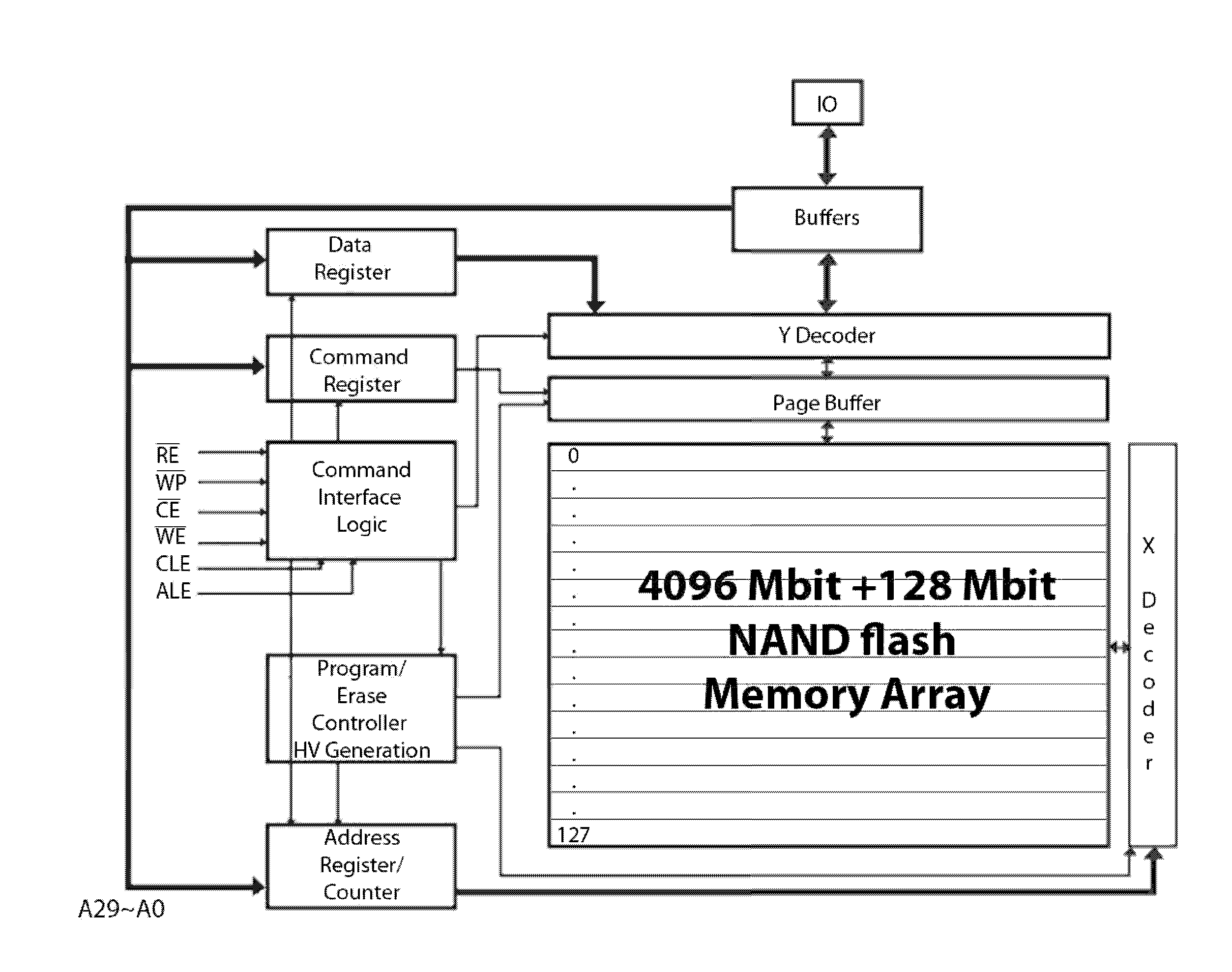
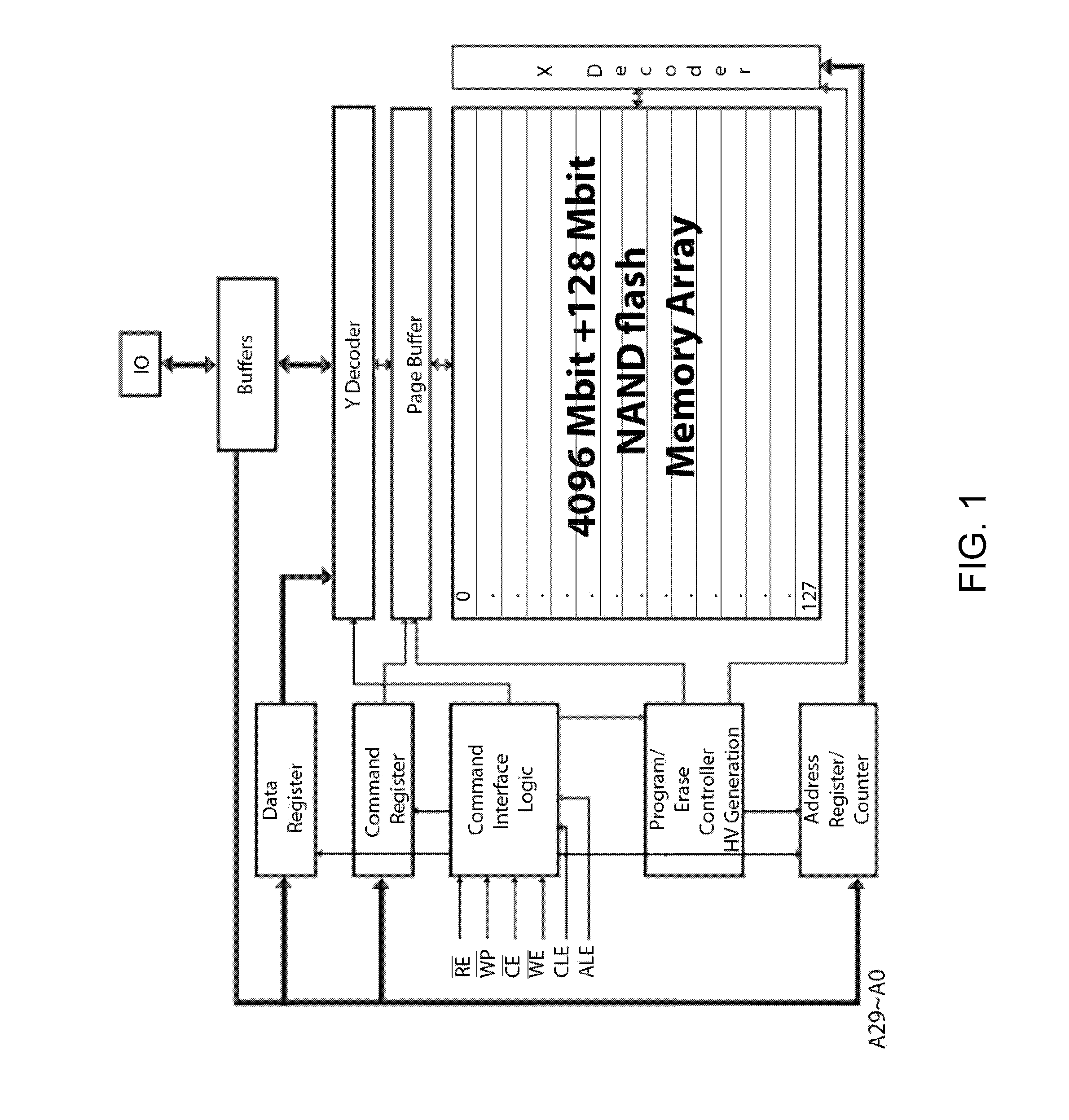
[0041]Though the present invention is generally directed to non-volatile memory-based mass storage devices, for example, solid-state drives (SSDs), that are capable of using a variety of non-volatile solid-state memory devices, the following discussion will refer specifically to mass storage devices that make use of NAND flash memory devices, in part because NAND flash memory is a non volatile memory at extremely low cost per Byte, which makes it extremely suitable for use in mass storage devices.

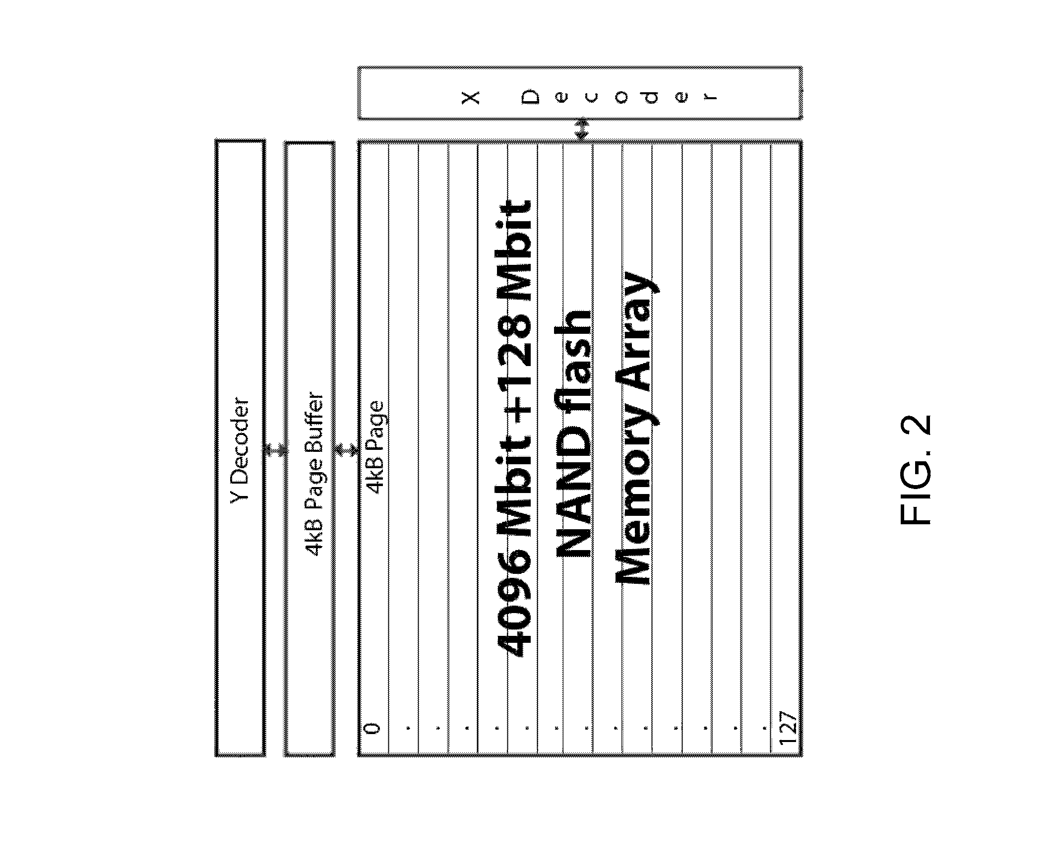
[0042]The internal architecture of NAND flash memory devices causes a few functional idiosyncrasies, for example, data always are written and read in the form of entire pages, a plurality of which forms a block, which in turn is the smallest functional unit for erasing data. For the purpose of the current invention, the organization of NAND flash memory devices into pages as the smallest functional unit for read and write accesses is particularly relevant.

[0043]Most modern file systems use ...


PUM


Abstract

Mass storage devices and methods that use at least one non-volatile solid-state memory device, for example, one or more NAND flash memory devices, that defines a memory space for permanent storage of data. The mass storage device is adapted to be operatively connected to a host computer system having an operating system and a file system. The memory device includes memory cells organized in pages that are organized into memory blocks for storing data, and a page buffer partitioned into segments corresponding to a cluster size of the operating system or the file system of the host computer system. The size of a segment of the page buffer is larger than the size of any page of the memory device. The page buffer enables logically reordering multiple clusters of data fetched into the segments from pages of memory device and write-combining segments containing valid clusters.

Description

BACKGROUND OF THE INVENTION[0001]The present invention generally relates to memory devices for use with computers and other processing apparatuses. More particularly, this invention relates to non-volatile (permanent) memory-based mass storage devices that use flash memory devices or any similar non-volatile solid-state memory devices for permanent storage of data.[0002]Mass storage devices such as advanced technology (ATA) or small computer system interface (SCSI) drives are rapidly adopting non-volatile solid-state memory technology such as flash memory or other emerging solid-state memory technology, including phase change memory (PCM), resistive random access memory (RRAM), magnetoresistive random access memory (MRAM), ferromagnetic random access memory (FRAM), organic memories, and nanotechnology-based storage media such as carbon nanofiber / nanotube-based substrates. Currently the most common technology uses NAND flash memory devices as inexpensive storage memory.[0003]NAND fla...

Claims


Application Information

Patent Timeline
Patent Type & Authority Applications(United States)
IPC IPC(8): G06F12/00
CPCG06F12/0246G06F2212/1016G06F2212/1044G06F2212/7201G06F2212/7203
Inventor JEONG, SOOGIL
Owner KK TOSHIBA
Why Eureka
Try Eureka