Utbb CMOS imager

a cmos imager and cmos technology, applied in the field of photodetection and imaging, can solve the problems of reducing collection efficiency and bulkiness

Active Publication Date: 2013-05-09
COMMISSARIAT A LENERGIE ATOMIQUE ET AUX ENERGIES ALTERNATIVES
View PDF6 Cites 5 Cited by
  • Summary
  • Abstract
  • Description
  • Claims
  • Application Information

AI Technical Summary

Benefits of technology

[0028]Such an assembling can be made without requiring an accurate aligning.

Problems solved by technology

Such an assembling requires an accurate aligning between the reading circuit and photodetector elements and gives rise to bulkiness problems.
During this transfer, part of the electrons can be recombined, which decreases the collection efficiency.
There arises the problem of implementing a new image sensor structure improved in relation with the drawbacks discussed above, in particular in terms of bulk.

Method used


Image

  • Utbb CMOS imager
  • Utbb CMOS imager
  • Utbb CMOS imager

Examples


Embodiment Construction

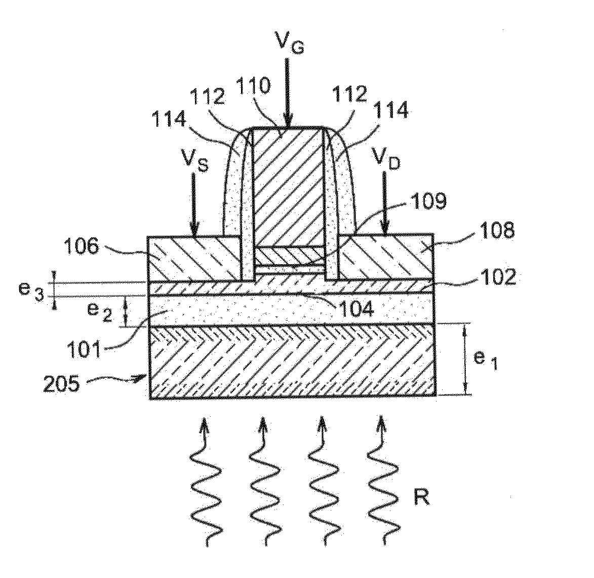
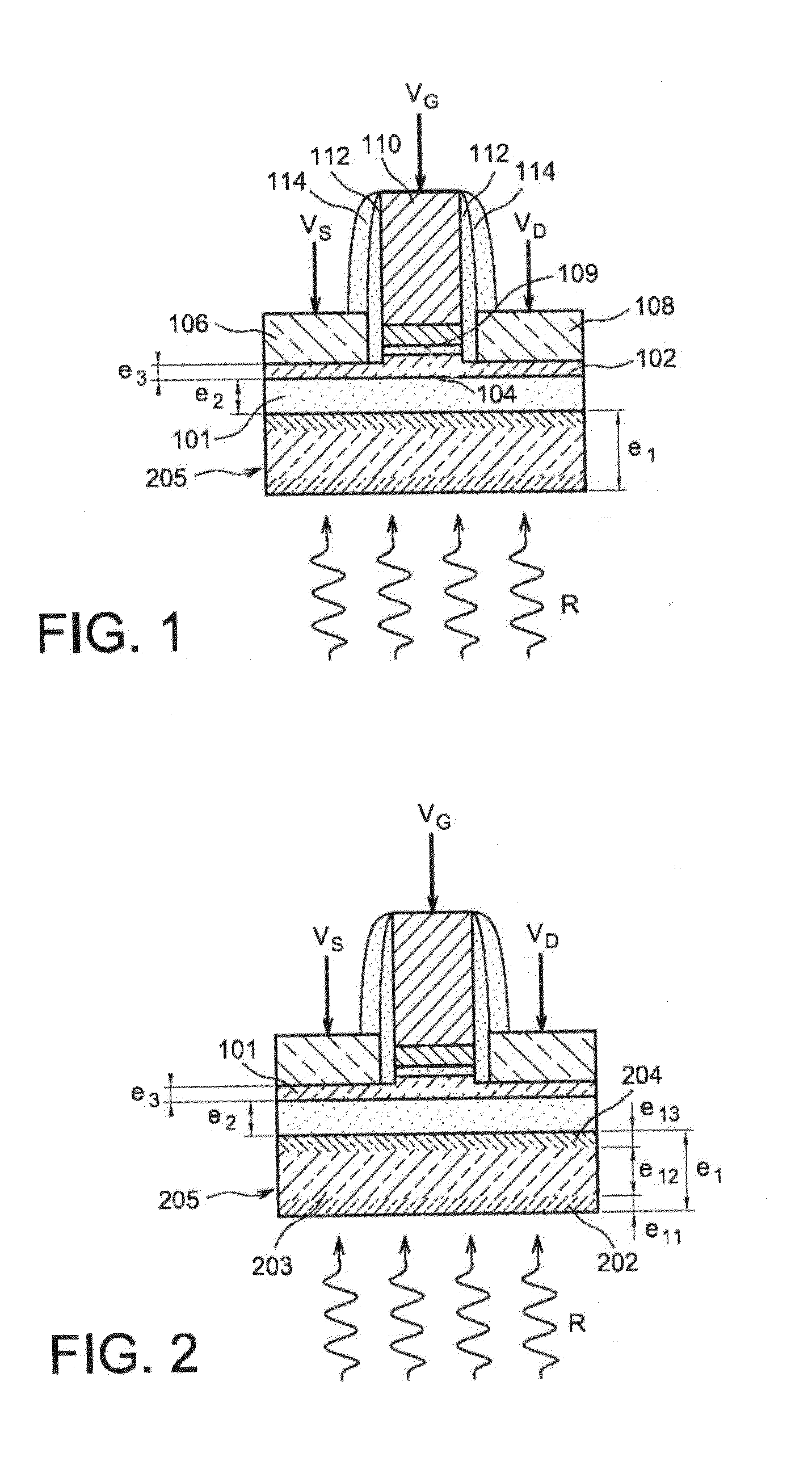
[0045]An exemplary single cell also called “pixel” of an image sensor device according to the invention will now be described in connection with FIGS. 1, 2 and 3.

[0046]This pixel comprises a photosensitive area 205 formed with at least two superimposed doped areas making a diode junction, for example a PN-type junction.

[0047]The thickness e1 of the photosensitive area and exposed to the radiation, can be set higher than 1 / a, a being the linear absorption coefficient of the material of the photosensitive area, in order to maximize the absorptions of photons in the photosensitive part, and in particular in the space charge area.

[0048]The thickness e1 of the photosensitive area can for example be between 100 nm and 10 μm, for example in the order of 1 μm.

[0049]The photodetecting area can have an area for example in the order of one μm2 for a wavelength detection for example in the order of one micrometer.

[0050]In the example given in FIG. 2, the photosensitive area 205 is in the form o...


PUM

PropertyMeasurementUnit
thicknessaaaaaaaaaa
thicknessaaaaaaaaaa
thicknessaaaaaaaaaa

Abstract

An image sensor device comprising at least one transistor lying on a semiconductor-on-insulator substrate, the substrate comprising a thin semi-conducting layer wherein a channel area of said transistor is made, an insulating layer separating the thin semi-conducting layer with a semi-conducting support layer, the device being characterized in that the semi-conducting support layer comprises at least one photosensitive area including at least one P-doped region and at least one N-doped region forming a junction provided facing the channel area of said transistor.

Description

TECHNICAL FIELD AND PRIOR ART[0001]The present invention relates to the field of photodetection and imaging and is concerned with the implementation of a imager device being improved in terms of arrangement and provided with a photodetection element and a reading element which are associated, wherein the signal transmission between the detection element and the reading element is simplified.[0002]An image sensor device can be formed with a matrix of photodetector elements which is connected and assembled with a reading electronic circuit by connecting elements. According to a known exemplary embodiment, these connecting elements can be indium beads. Such an assembling requires an accurate aligning between the reading circuit and photodetector elements and gives rise to bulkiness problems.[0003]In a CMOS type image sensor device, pixels are generally formed with a photodetector element such as a photodiode for example of the type commonly called “pinned”, and with a reading element, ...

Claims


Application Information

Patent Timeline
Patent Type & Authority Applications(United States)
IPC IPC(8): H01L27/146H01L31/18
CPCH01L27/146H01L31/18H01L27/1461H01L27/14694H01L27/14632H01L27/14636H01L27/1464H01L27/14612
Inventor GRENOUILLET, LAURENTVINET, MAUD
Owner COMMISSARIAT A LENERGIE ATOMIQUE ET AUX ENERGIES ALTERNATIVES
Why Eureka
Try Eureka