
Field emission devices including nanotubes or other nanoscale articles

a field emission device and carbon nanotube technology, applied in the manufacture of electrode systems, electric discharge tubes/lamps, discharge tubes luminescnet screens, etc., can solve the problems of high fabrication cost, limited current technology, and field emission

Inactive Publication Date: 2013-05-09
MASSACHUSETTS INST OF TECH
View PDF5 Cites 19 Cited by
  • Summary
  • Abstract
  • Description
  • Claims
  • Application Information

AI Technical Summary

Benefits of technology

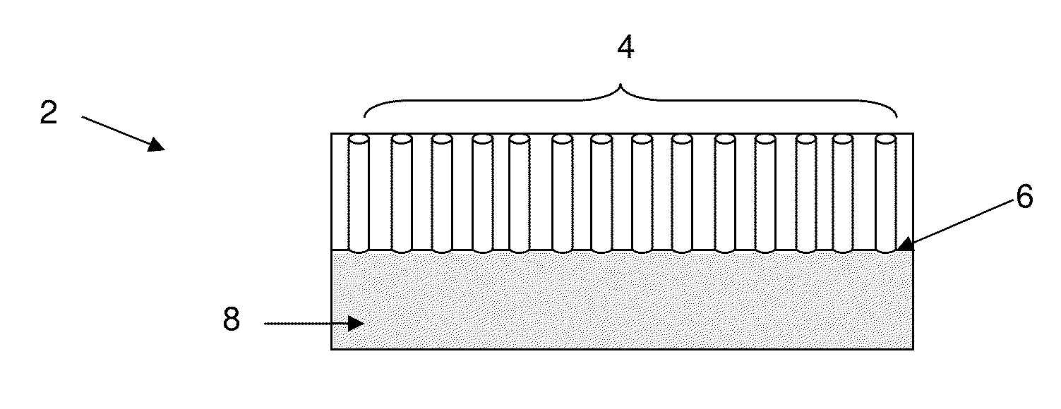
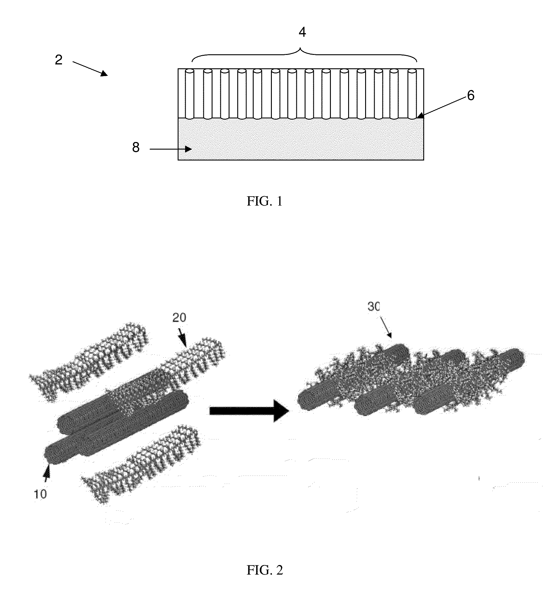
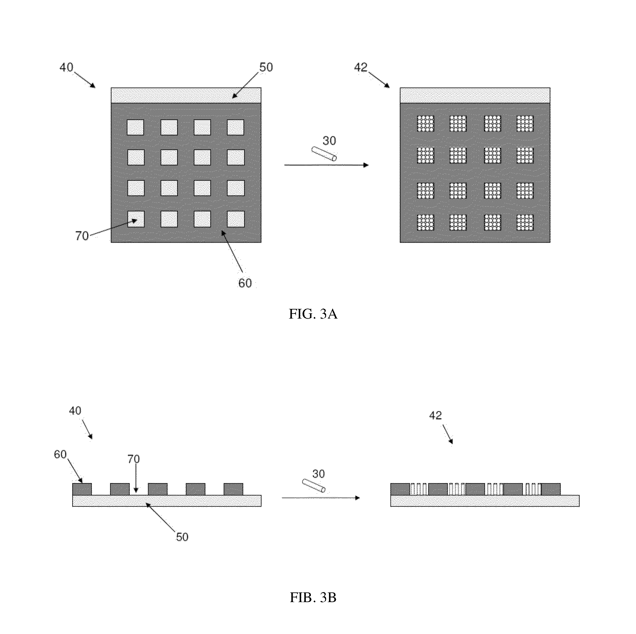
The present invention relates to devices and methods using carbon nanotubes in field emission devices. The invention includes the use of a polymer support material that contains carbon nanotubes and the orientation of the carbon nanotubes in relation to the substrate surface. The invention also includes the use of an electric field to align the carbon nanotubes with the substrate surface. These features improve the performance and efficiency of field emission devices. The technical effects of the invention include improved field emission devices and methods of their use.

Problems solved by technology

Application of a voltage across the electrodes can cause an emission of electrons from electron-emitting material, which may be used to excite the light-emitting material, resulting in a field emission.
Although methods have been utilized to incorporate carbon nanotubes within FEDs, current technology may have some limitations.
While this may allow for control over the average orientation of the nanotubes on a surface, fabrication may be high in cost.
Also, growth of carbon nanotubes over a large surface area can be difficult due to incompatibility between the stability of the substrate material and the conditions required for carbon nanotube growth.
However, using this method, it may be difficult to control the density and orientation of the carbon nanotubes in the resulting structure.
Also, the filler material may reduce the lifetime and stability of the carbon nanotubes.

Method used


Image

  • Field emission devices including nanotubes or other nanoscale articles
  • Field emission devices including nanotubes or other nanoscale articles
  • Field emission devices including nanotubes or other nanoscale articles

Examples


example 1

[0058]Single-walled carbon nanotubes were purchased from Carbon Nanotechnologies Inc. (CNI Lot #R0204). The carbon nanotubes were combined with high molecular weight poly(3-hexylthiophene), a polymeric surfactant, to form a stable carbon nanotube suspension. Next, an anode and a cathode (e.g., a gold cathode), spaced 1-2 mm apart, were immersed within the suspension, as shown by the photograph in FIG. 5A. Using an Autolab electrochemical station, a DC bias voltage (5 V) was applied to the suspension and substrate for nanotube deposition, with the cathode serving as the substrate. The deposition speed was 4 microns / second.

[0059]The absorption spectrum of the assembly of carbon nanotubes was measured between two ITO slides. FIG. 6A shows the UV-visible absorption spectra of the assembly of carbon nanotubes after (a) 0 minutes, (b) 1 minute, (c) 10 minutes, and (d) 20 minutes of electrophoretic deposition on the substrate. FIG. 6B shows the near-IR absorption spectra of an assembly of ...

example 2

[0061]The resistance of a carbon nanotube assembly formed by electrophoretic deposition as described herein was compared to the resistance of a carbon nanotube assembly formed by spin-coating. The electrophoretically deposited assembly had a resistance of 30 Ohms, while the spin-coated assembly exhibited a resistance of approximately 3000 Ohms. Thus, the resistance of the electrophoretically deposited assembly comprising a high degree of aligned carbon nanotubes was 100 times greater than the spin-coated assembly comprising a relatively lower degree of aligned carbon nanotubes.


PUM

PropertyMeasurementUnit
voltageaaaaaaaaaa
surface areaaaaaaaaaaa

Abstract

The present invention provides devices comprising an assembly of carbon nanotubes, and related methods. In some cases, the carbon nanotubes may have enhanced alignment. Devices of the invention may comprise features and / or components which may enhance the emission of electrons and may lower the operating voltage of the devices. Using methods described herein, carbon nanotube assemblies may be manufactured rapidly, at low cost, and over a large surface area. Such devices may be useful in display applications such as field emission devices, or other applications requiring high image quality, low power consumption, and stability over a wide to temperature range.

Description

STATEMENT REGARDING FEDERALLY SPONSORED RESEARCH OR DEVELOPMENT[0001]This invention was made with the support under the following government contract: N000140310897 awarded by the Office of Naval Research. The government has certain rights in the invention.FIELD OF THE INVENTION[0002]The present invention relates to devices comprising carbon nanotubes including field emission devices, and related methods.BACKGROUND OF THE INVENTION[0003]A field emission device (FED) is generally considered to be a device in which an electron beam is focused between two electrodes, producing a field emission. Typically, the FED may include an electron-emitting material and a light-emitting material. Application of a voltage across the electrodes can cause an emission of electrons from electron-emitting material, which may be used to excite the light-emitting material, resulting in a field emission. Generally, the efficiency of electron emission may depend on the material utilized as the electron emit...

Claims


Application Information

Patent Timeline
Patent Type & Authority Applications(United States)
IPC IPC(8): H01J1/304
CPCB82Y99/00H01J1/3042H01J1/304H01J9/025H01J63/06H01J2201/30469H01J2329/0455B82Y10/00H01J63/02
Inventor SWAGER, TIMOTHY M.GU, HONGWEI
Owner MASSACHUSETTS INST OF TECH
Learn More