Plasma processing apparatus and plasma processing method

a plasma processing apparatus and plasma technology, applied in the direction of program control, instruments, semiconductor/solid-state device testing/measurement, etc., can solve the problems of adversely affecting process performance, inconvenient fluctuation of process performance results, and inability to obtain desired processing performance, etc., to achieve stable process performance results

Active Publication Date: 2013-05-16
HITACHI HIGH-TECH CORP
View PDF6 Cites 170 Cited by
  • Summary
  • Abstract
  • Description
  • Claims
  • Application Information

AI Technical Summary

Benefits of technology

[0018]The present invention has the construction described above, thus allowing plasma processing to be carried out by Run-to-Run cont

Problems solved by technology

In the aforesaid plasma processing apparatus, with scaling down of semiconductor devices, it has been becoming difficult to obtain desired processing performance (hereinafter referred to as “process performance”) each time due to various disturbances even if the processing is carried out under the same manufacturing condition (hereinafter referred to as “recipe”).
However, the process performance results (e.g., etching rate, processing dimensions or the like in the case of a plasma etching apparatus) inconveniently fluctuate with time in some cases due to substances adhering to the inner wall of a plasma etching chamber, or changes in the wear on components in the plasma etching chamber.
In the Run-to-Run control, carrying out plasma processing according to a particular recipe that has a parameter exceeding a predetermined range may adv

Method used


Image

  • Plasma processing apparatus and plasma processing method
  • Plasma processing apparatus and plasma processing method
  • Plasma processing apparatus and plasma processing method

Examples


Embodiment Construction

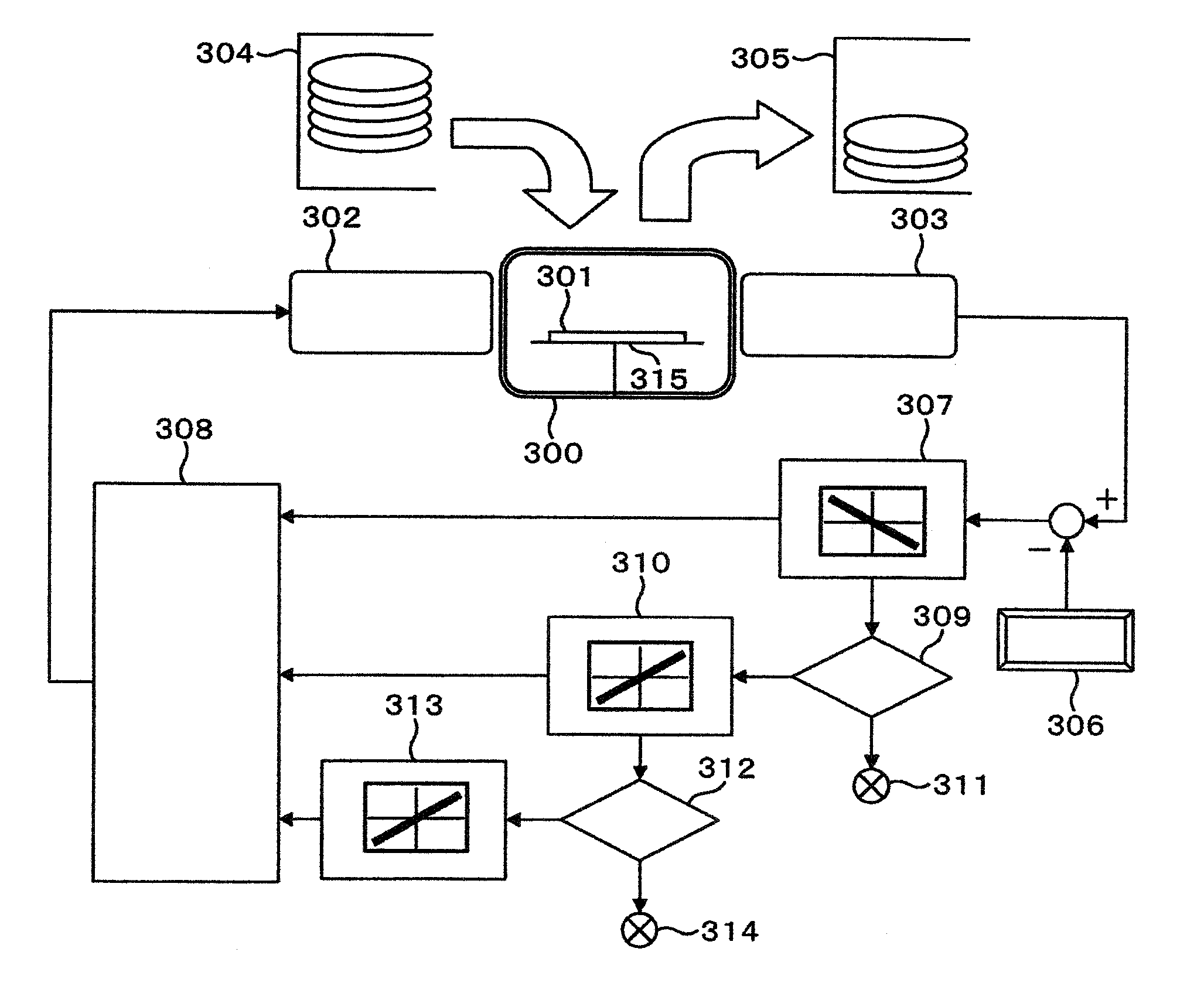
[0031]With reference to the accompanying drawings, the following will describe a mode, in which Run-to-Run control is conducted in a plasma etching apparatus, as a best mode to carry out the present invention.

[0032]There are a variety of processes of plasma etching processing, depending on materials to be etched, such as a silicon material and an insulating material. In the present embodiment, etching of a silicon nitride layer will be described as an example.

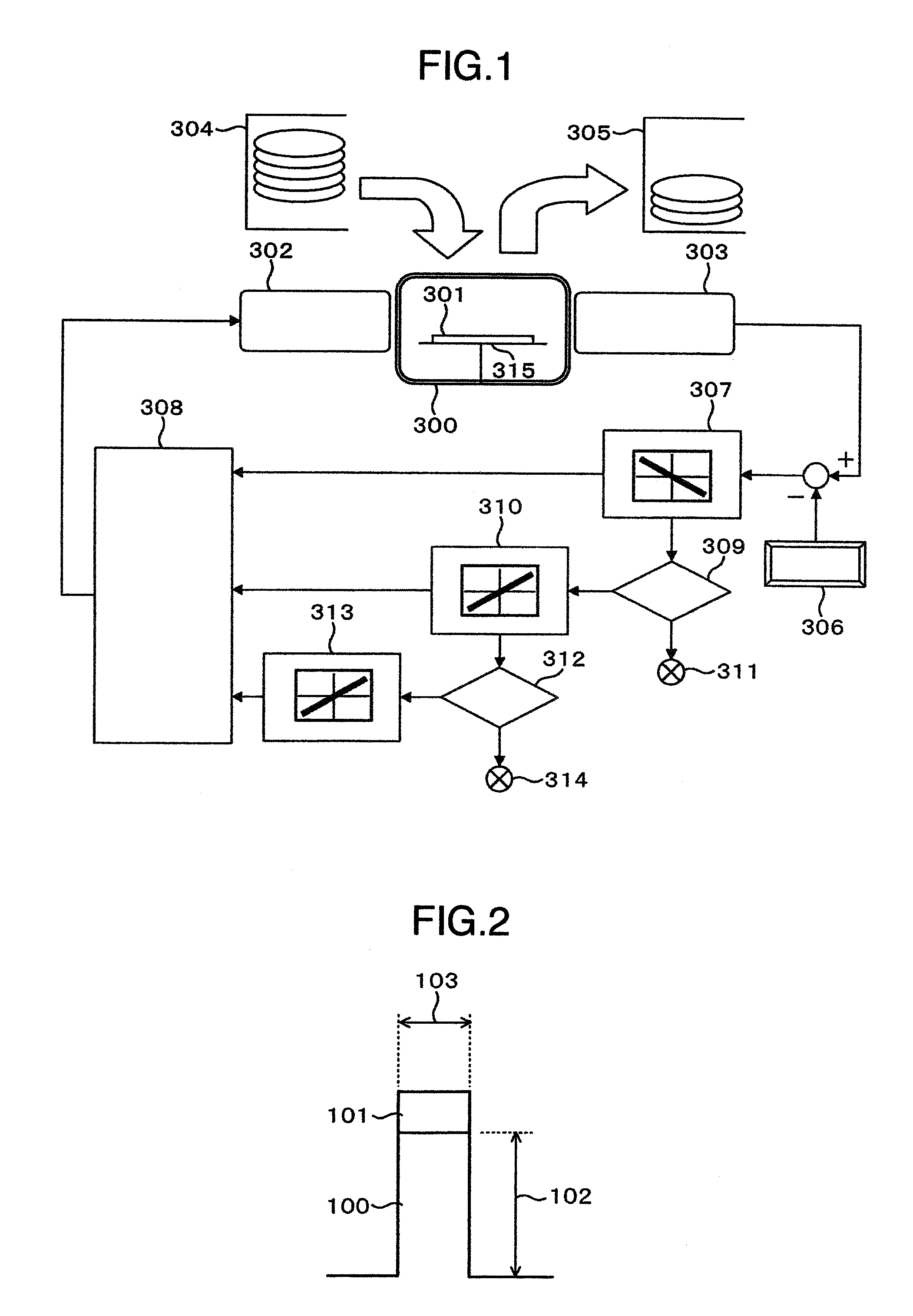
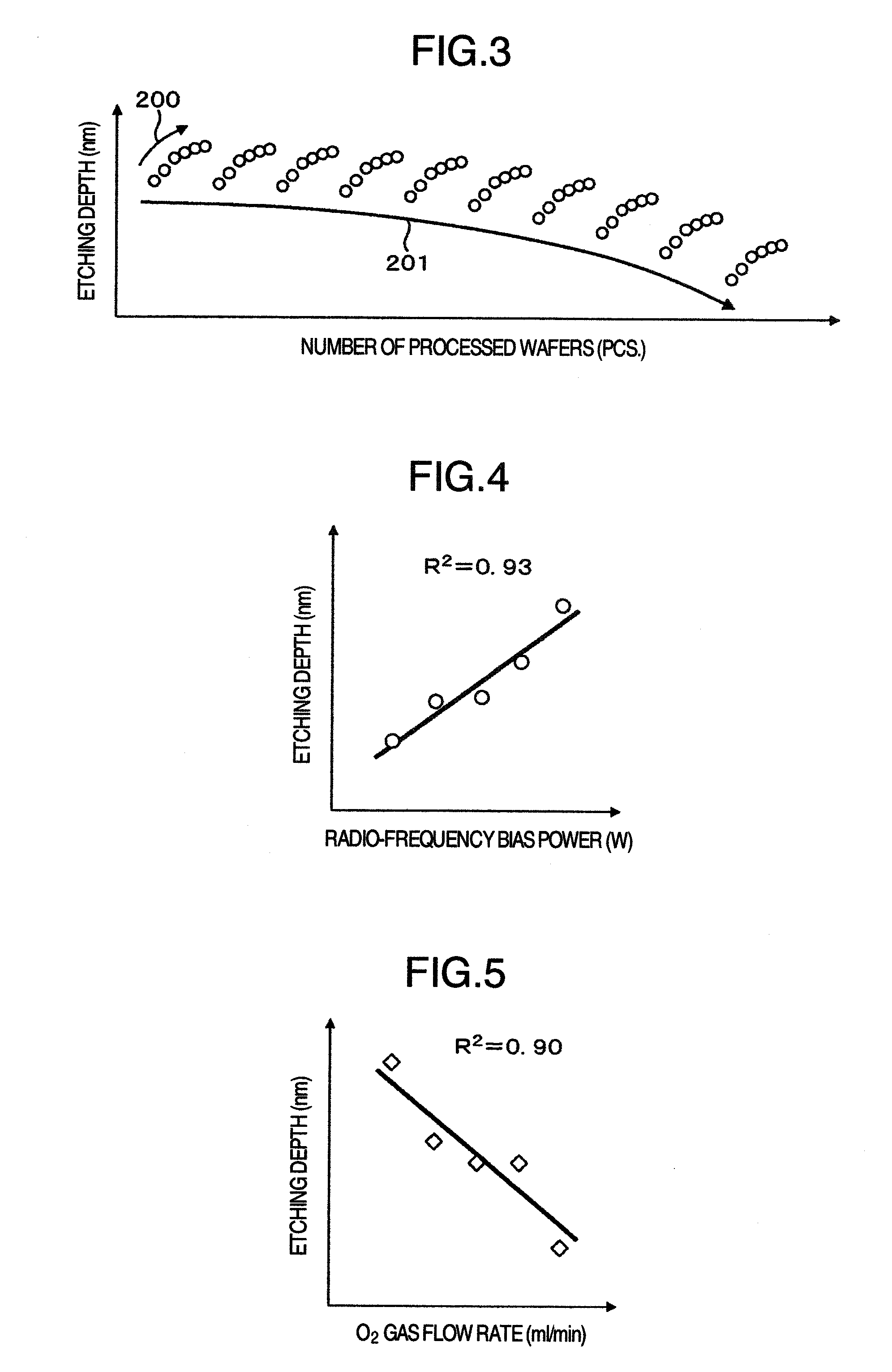
[0033]FIG. 2 illustrates a simple example of etching a silicon nitride layer. The etching process of the silicon nitride layer is a process whereby to etch a silicon nitride layer 100 by using a mask material 101 as the mask. A gas for etching the silicon nitride layer may be, for example, a mixed gas of methyl fluoride gas (CH3F gas) and oxygen gas (O2 gas), as shown in Table 1. Indexes for assessing etching performance typically include an etching depth 102 and a critical dimension (CD), such as a processing dimension 103. In...


PUM

PropertyMeasurementUnit
Flow rateaaaaaaaaaa

Abstract

A plasma processing apparatus includes a plasma processing chamber, a process monitor which monitors a condition in the plasma processing chamber, an actuator which controls a parameter constituting a plasma processing condition, N+1 correction amount calculating units which calculate a correction amount of a manipulated variable on the basis of a difference between a process monitor value monitored by the process monitor and a desired value of the process monitor and a correlation between the process monitor value and a manipulated variable, which is the parameter, the correlation having been acquired in advance, and N manipulated variable adding units that add a manipulated variable having a priority level next to an N-th manipulated variable. The N-th manipulated variable adding unit defines a correction amount calculated by the N+1-th correction amount calculating unit as the correction amount of an N+1-th manipulated variable.

Description

BACKGROUND OF THE INVENTION[0001](1) Field of the Invention[0002]The present invention relates to a plasma processing apparatus and a plasma processing method and, more particularly, to a plasma processing apparatus and a plasma processing method that make it possible to restrain influences attributable to fluctuations in process performance, which occur as plasma processing proceeds.[0003](2) Description of Related Art[0004]As a plasma processing apparatus, there has been known, for example, a plasma etching apparatus adapted to introduce an etching gas into a vacuum processing chamber to generate plasma under reduced pressure and to cause radicals or ions generated by the plasma to react with a wafer surface, which is an object to be processed, thereby accomplishing plasma etching.[0005]In the aforesaid plasma processing apparatus, with scaling down of semiconductor devices, it has been becoming difficult to obtain desired processing performance (hereinafter referred to as “proces...

Claims


Application Information

Patent Timeline
IPC IPC(8): H05H1/24B44C1/22
CPCH01J37/32935H01J2237/3343H01J37/3299H01J37/32449H01J37/32926H01L21/3065G05B13/00G05B13/021G05B13/042G05B19/4184H01L22/20H01L22/26
Inventor KAGOSHIMA, AKIRASHIRAISHI, DAISUKENAGATANI, YUJI
Owner HITACHI HIGH-TECH CORP
Why Eureka
Try Eureka