Semiconductor device and manufacturing method thereof

a technology of semiconductors and semiconductors, applied in non-linear optics, instruments, optics, etc., can solve the problem of unintentional portion acting as transistors, and achieve the effect of reducing the number of photolithography processes used for manufacturing transistors, high productivity and low cos

Inactive Publication Date: 2013-05-30
SEMICON ENERGY LAB CO LTD
View PDF24 Cites 16 Cited by
  • Summary
  • Abstract
  • Description
  • Claims
  • Application Information

AI Technical Summary

Benefits of technology

[0055]With an embodiment of the present invention, the number of photolithography processes used for manufacturing a transistor can be reduced to less than the conventional one. This enables the number of photomasks used for manufacturing a semiconductor device including a transistor to be reduced to less than the conventional one. Thus, a semiconductor device can be provided with high productivity and low cost. Further, a display device using the semiconductor device can be provided with high productivity and low cost.
[0056]In an embodiment of the present invention, an oxide semiconductor is used for a semiconductor layer in which a channel is formed, whereby a semiconductor device with low power consumption and high reliability can be provided. Further, a highly reliable display device that uses the semiconductor device can be provided.
[0057]In an embodiment of the present invention, a layer formed using an oxide insulating material containing at least one of In and Zn is formed in contact with a semiconductor layer, in which case the interface between the layer and the semiconductor layer can be kept in a favorable state. Thus, favorable transistor characteristics can be obtained. Further, by using the transistor, a highly reliable semiconductor device with stable electrical characteristics can be provided.
[0058]In an embodiment of the present invention, a layer of an oxide semiconductor having a higher insulating property than the semiconductor layer is formed over or under the semiconductor layer. Thus, variation in threshold voltage due to charge buildup of the insulating layer can be suppressed and deterioration in transistor characteristics or damage to the transistor due to static electricity can be prevented. Thus, by using the transistor, a semiconductor device can be manufactured at high yield, so that productivity of the semiconductor device can be improved.

Problems solved by technology

However, the reduction in the number of photolithography processes or the simplification of the photolithography process may cause a channel to be formed in a place where the channel is essentially unnecessary; therefore, an unintentional portion may function as a transistor.

Method used


Image

  • Semiconductor device and manufacturing method thereof
  • Semiconductor device and manufacturing method thereof
  • Semiconductor device and manufacturing method thereof

Examples


embodiment 1

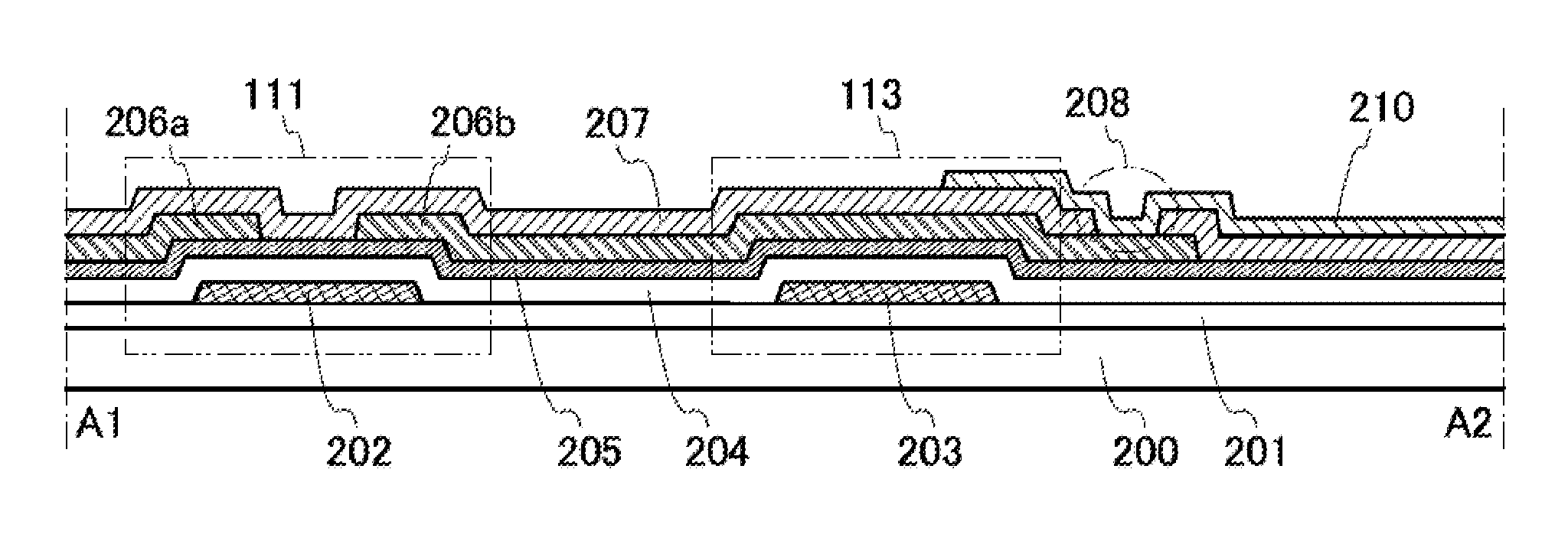
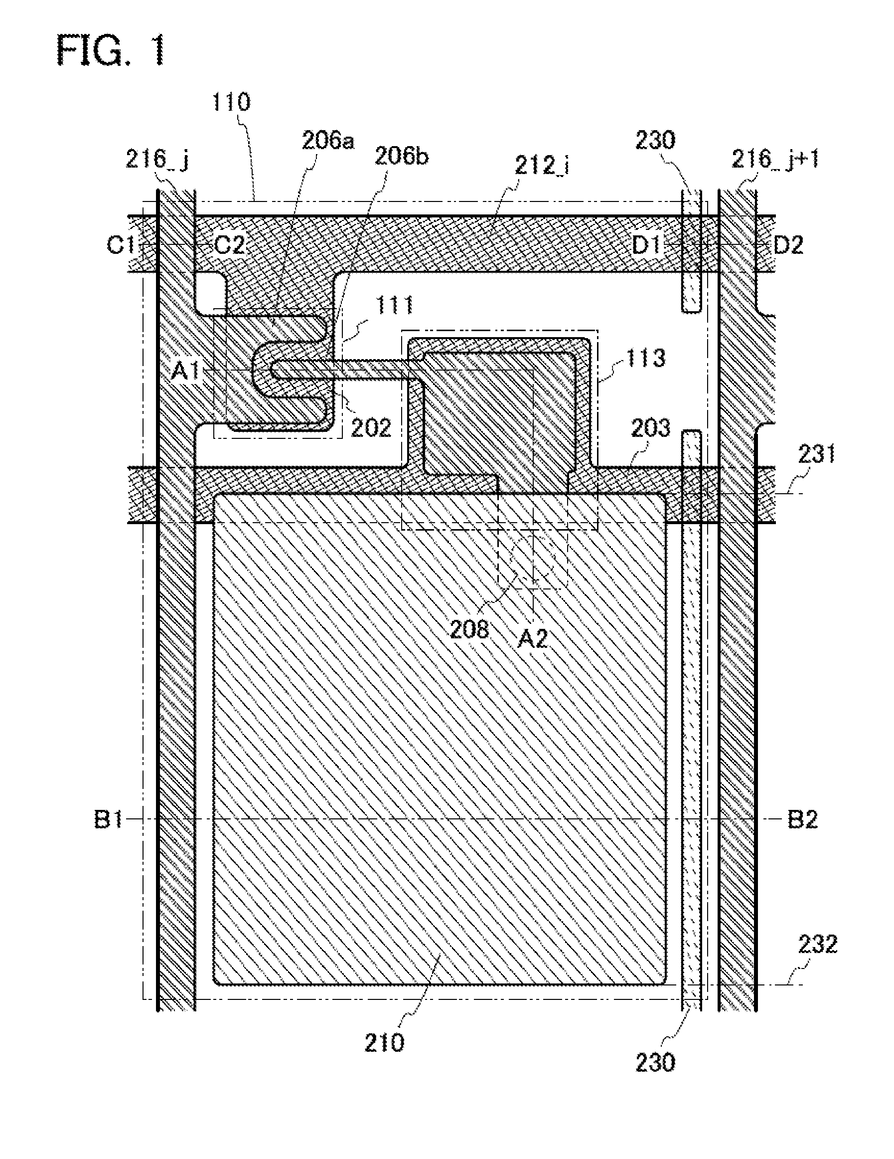
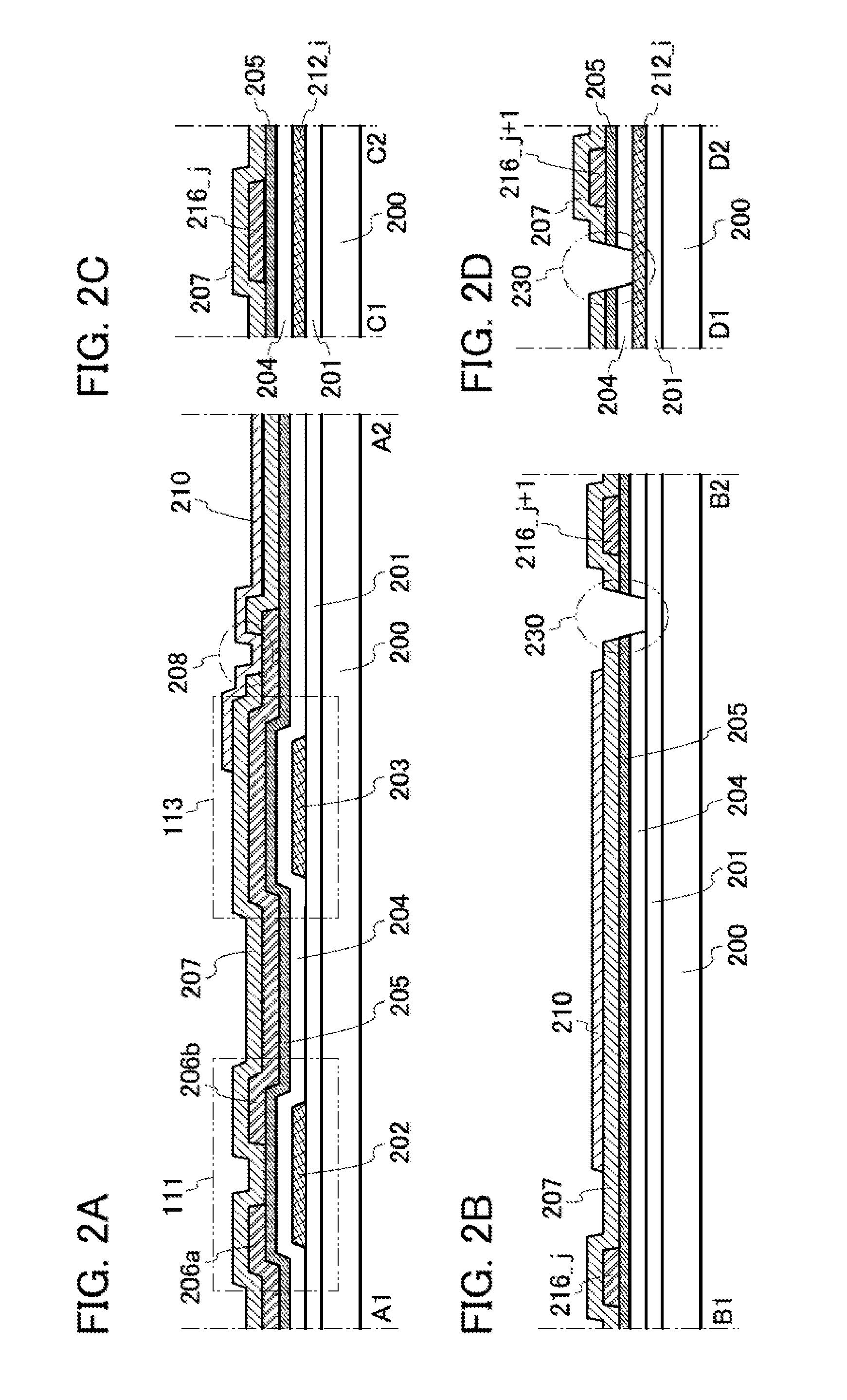
[0089]In this embodiment, as an example of a semiconductor device formed through a process in which the number of photomasks and the number of photolithography processes are reduced, an example of a semiconductor device that can be used in an active matrix liquid crystal display device and a manufacturing method thereof will be described with reference to FIG. 1 to FIG. 10C.

[0090]FIG. 6A illustrates an example of the configuration of a semiconductor device 100 that can be used in a liquid crystal display device. The semiconductor device 100 includes a pixel region 102, terminal portions 103 each including m terminals 105_1 to 105—m (m is an integer of greater than or equal to 1) and a terminal 107, and terminal portions 104 each including n terminals 106_1 to 106—n (n is an integer of greater than or equal to 1) over a substrate 101. Further, the semiconductor device 100 includes m wirings 212_1 to 212—m and wirings 203 that are electrically connected to the terminal portions 103, a...

embodiment 2

[0287]An embodiment of a liquid crystal display device that uses the semiconductor device described in Embodiment 1 is illustrated in FIGS. 11A and 11B.

[0288]FIG. 11A is a plan view of a panel in which a transistor 4010 and a liquid crystal element 4013 are sealed between a first substrate 4001 and a second substrate 4006 with a sealant 4005. FIG. 11B is a cross-sectional view taken along line M1-M2 in FIG. 11A. A groove portion 4040 is provided over the first substrate 4001.

[0289]The sealant 4005 is provided so as to surround a pixel portion 4002 provided over the first substrate 4001, and the second substrate 4006 is provided over the pixel portion 4002. Accordingly, the pixel portion 4002 is sealed together with a liquid crystal layer 4008 by the first substrate 4001, the sealant 4005, and the second substrate 4006.

[0290]Further, an input terminal 4020 is provided in a region over the first substrate 4001 and outside a region surrounded by the sealant 4005, and flexible printed c...

embodiment 3

[0322]In this embodiment, as an example of a semiconductor device formed through a process in which the number of photomasks and the number of photolithography processes are reduced, an example of a semiconductor device that can be used in an active matrix EL display device and a manufacturing method thereof will be described with reference to FIG. 12 to FIGS. 19A to 19C.

[0323]An example of the configuration of a semiconductor device 150 that can be used in an EL display device will be described with reference to FIG. 17A. The semiconductor device 150 includes a pixel region 102, terminal portions 103 each including m terminals 105_1 to 105—m (m is an integer of greater than or equal to 1) and a terminal 107, and terminal portions 104 each including n terminals 106_1 to 106—n (n is an integer of greater than or equal to 1) and a terminal 108, over a substrate 101. Further, the semiconductor device 150 includes m wirings 212_1 to 212—m electrically connected to the terminal portions ...


PUM


Abstract

A step for forming an island-shaped semiconductor layer of a semiconductor device used in a display device is omitted in order to manufacture the semiconductor device with high productivity and low cost. The semiconductor device is manufactured through four photolithography processes: four steps for forming a gate electrode, for forming a source electrode and a drain electrode, for forming a contact hole, and for forming a pixel electrode. In the step for forming the contact hole, a groove portion in which a semiconductor layer is removed is formed, whereby formation of a parasitic transistor is prevented. An oxide semiconductor is used as a material of the semiconductor layer in which a channel is formed, and an oxide semiconductor having a higher insulating property than the semiconductor layer is provided over the semiconductor layer.

Description

BACKGROUND OF THE INVENTION[0001]1. Field of the Invention[0002]The present invention relates to a semiconductor device and a manufacturing method thereof.[0003]In this specification, a semiconductor device means all types of devices that can function by utilizing semiconductor characteristics, and a transistor, a semiconductor circuit, a memory device, an imaging device, a display device, an electro-optical device, an electronic device, and the like are all semiconductor devices.[0004]2. Description of the Related Art[0005]In recent years, transistors that are formed using a semiconductor thin film having a thickness of several nanometers to several hundreds of nanometers over a substrate having an insulating surface such as a glass substrate have been attracting attentions. Transistors are widely used for electronic devices such as ICs (integrated circuits) and electro-optical devices. In particular, transistors are urgently developed as switching elements of image display devices...

Claims


Application Information

Patent Timeline
Patent Type & Authority Applications(United States)
IPC IPC(8): H01L29/786H01L29/66H05B44/00
CPCH01L29/7869H01L29/66969H01L27/1259H01L21/02565H01L21/44H01L27/1225H10K59/1315H10K59/131H01L27/1255H01L27/1288G02F1/136227H01L27/127H01L27/124H01L27/1262G02F1/13625G02F1/136231G02F1/136295H10K59/123
Inventor YAMAZAKI, SHUNPEIKOYAMA, JUN
Owner SEMICON ENERGY LAB CO LTD
Why Eureka
Try Eureka