Probe assembly for inspecting power semiconductor devices and inspection apparatus using the same

Active Publication Date: 2013-06-06
NIHON MICRONICS
View PDF6 Cites 13 Cited by
  • Summary
  • Abstract
  • Description
  • Claims
  • Application Information

AI Technical Summary

Benefits of technology

[0020]In a preferable embodiment, the probe assembly of the present invention equips a temperature sensor which measures the temperature of the probe block, thereby the temperature of the probe block is constantly monitored to know the temperature of the probes which are thermally contact with the probe block. Further, in another preferable embodiment, the probe assembly of the present invention has a control unit which regulates the action of a cooling means based on the output signals from the temperature sensor to control the temperature of the probe block. Therefore, according to the probe assembly of the present invention, it is possible to conduct characteristics inspection of a power semiconductor devices always at the most appropriate temperature.
[0021]According to the probe assembly of the present invention, the temperature rises of the probes and a power semiconductor device under test are suppressed even when a larger electric current is applied to the power semiconductor device throug

Problems solved by technology

The heat thus generated tends to invite temperature drift which disturbs accurate measurements, and damage the semiconductor device and/or inspection probes in some cases.
However, characteristic faults are frequently found in a final full-spec inspection on some of the power semiconductor devices which passed characteristics inspections conducted by applying small electric current.
In that case, various processes carried out after the rough selection become useless, which invites disadvantages such as products cost rising and waste volume increasing.
The cooling means, however, is equipped in the probe card not to prevent probes or a semiconductor device from being heated by large electric current applied to the semiconductor devic

Method used


Image

  • Probe assembly for inspecting power semiconductor devices and inspection apparatus using the same
  • Probe assembly for inspecting power semiconductor devices and inspection apparatus using the same
  • Probe assembly for inspecting power semiconductor devices and inspection apparatus using the same

Examples


Embodiment Construction

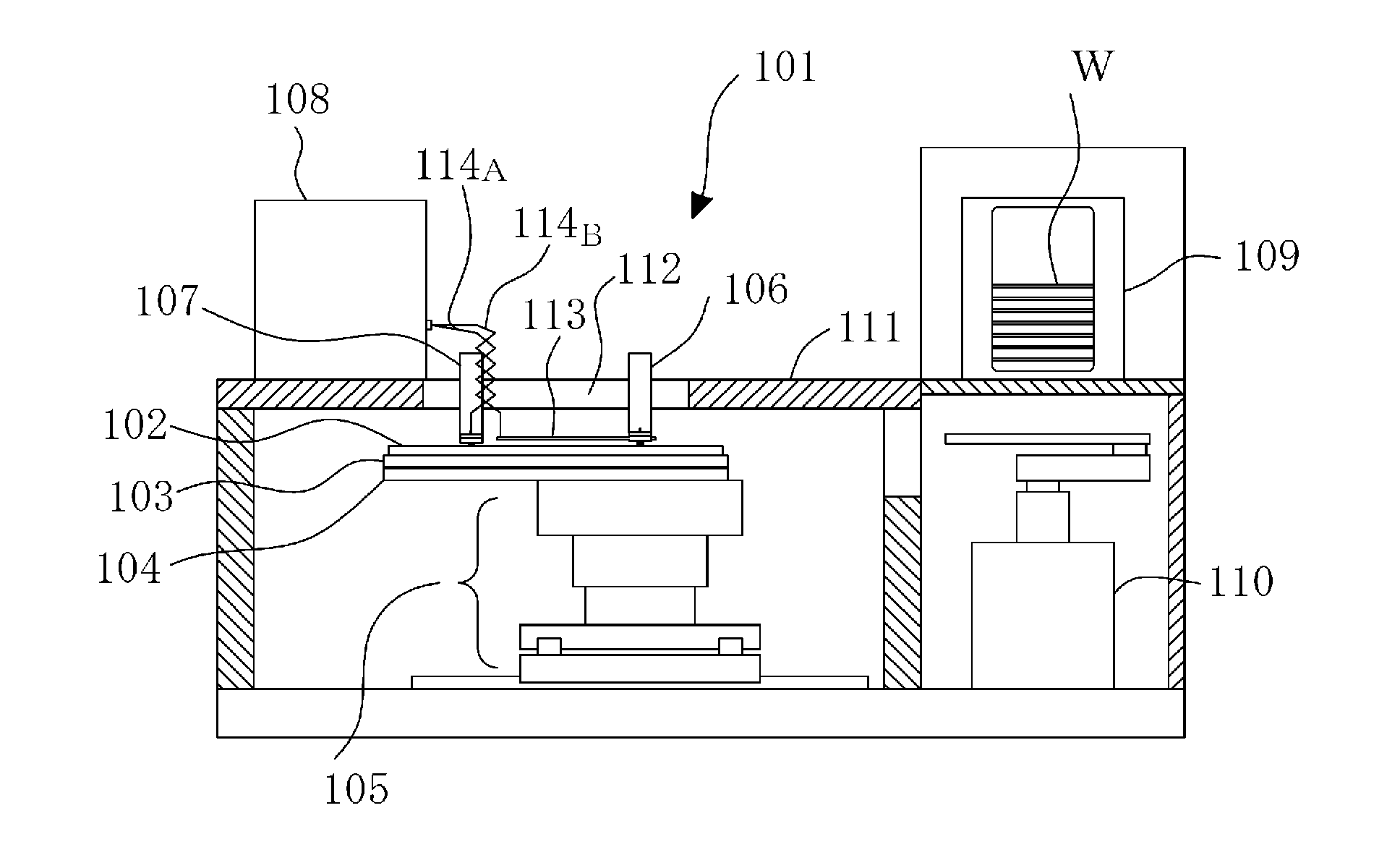
[0042]Hereinafter, the present invention is explained in detail with reference to the accompanying drawings picking up IGBT as an example of power semiconductor devices, which are the targets of the probe assembly and the inspection apparatus of the present invention. As a matter of course, the power semiconductor devices targeted by the present invention are not limited to IGBT, and the present invention is not limited to the illustrated examples.

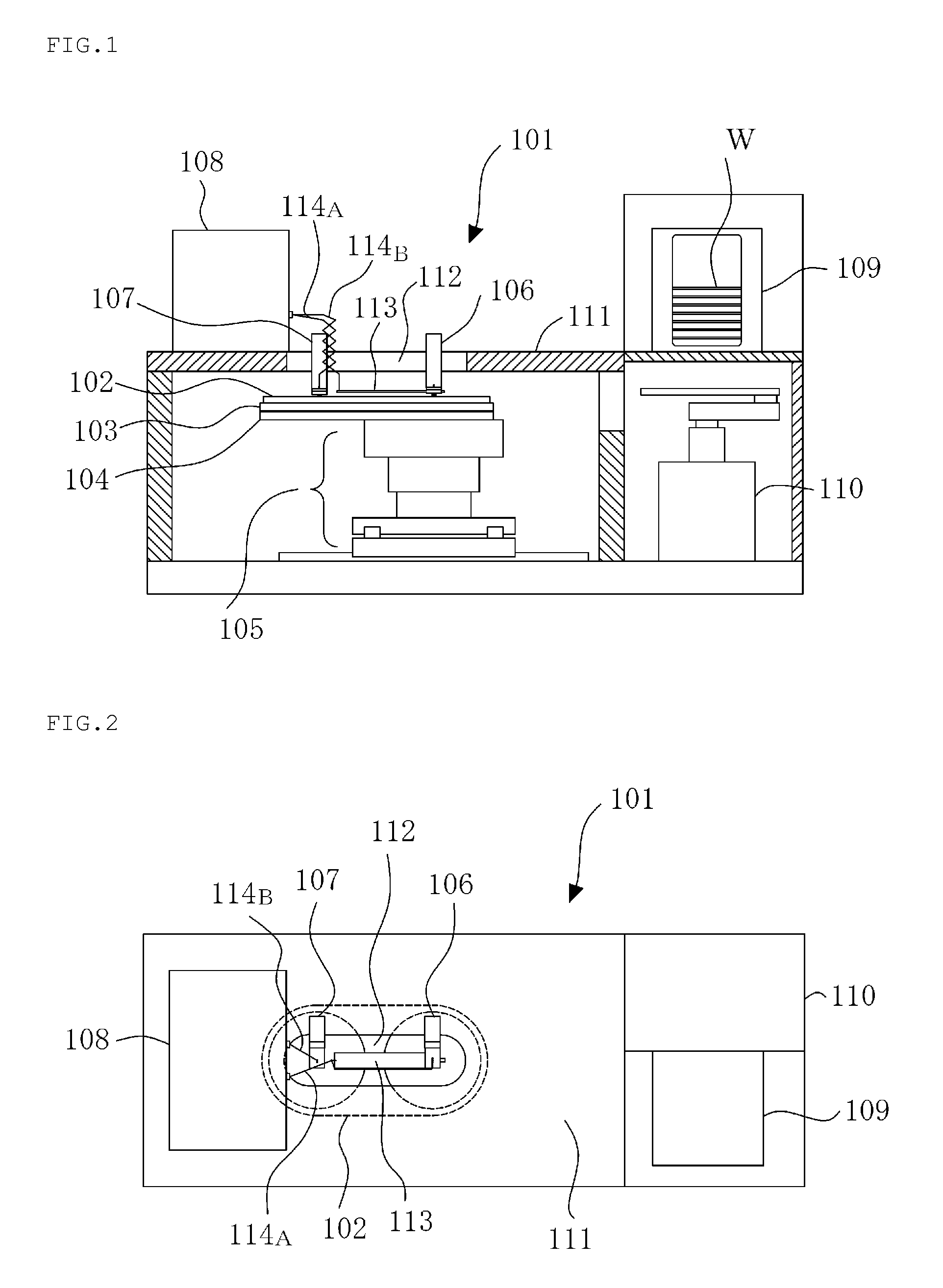
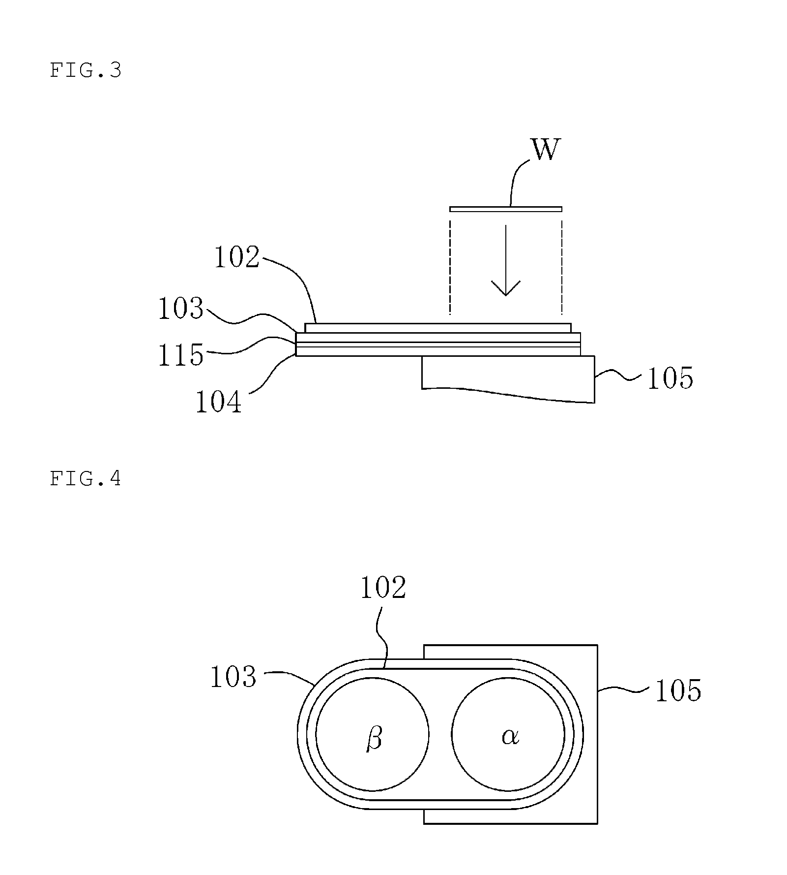
[0043]FIG. 1 is a partial cross section of a front view showing an example of an inspection apparatus for power semiconductor devices having a probe assembly according to the present invention. FIG. 2 is a plane view of the inspection apparatus as shown in FIG. 1. In FIG. 1 and FIG. 2, the reference numeral 101 indicates the inspection apparatus for power semiconductor devices, the reference numeral 102 indicates a chuck stage, the reference numeral 103 indicates an electric insulating plate on which the chuck stage 102 is placed and held,...


PUM


Abstract

The present invention provides a probe assembly for inspecting power semiconductor devices, which comprises (1) a probe block having more than one probe holding hole, (2) more than one probe, each of which is contained in one of the probe holding holes with its outer surface being in contact with the inner surface of the probe holding hole, and which has lower end protruding from the probe block and coming into contact with the power semiconductor device on inspection, and (3) one or more cooling means which cool the probe block. According to the probe assembly and the inspection apparatus having the prove assembly of the present invention, it is possible to inspect characteristics of power semiconductor devices accurately by suppressing temperature rises of the probes as well as the power semiconductor device under test.

Description

BACKGROUND OF THE INVENTION[0001]1. Field of the Invention[0002]The present invention relates to a probe assembly for inspecting power semiconductor devices and an inspection apparatus for power semiconductor devices using the probe assembly.[0003]2. Description of the Related Art[0004]For inspecting electric characteristics of power semiconductor devices, such as power transistor and IGBT (Insulated Gate Bipolar Transistor), it is preferable as a matter of course to apply large electric current at a level of several hundreds amperes to the device under test adapting to its actual operating conditions. However, when a large electric current is applied through inspection probes to a power semiconductor device in wafer state or in chip state after dicing, the semiconductor device and / or the inspection probes generate heat because of internal resistance of the semiconductor device and contact resistance found at the contact points of electrodes of the semiconductor device and the probe...

Claims


Application Information

Patent Timeline
IPC IPC(8): G01R1/067
CPCG01R1/067G01R31/2608G01R1/44G01R1/06777G01R31/2877G01R31/26
Inventor YASUTA, KATSUOMASUTA, HIKARUNEI, HIDEKIISHIWATARI, TATSUYA
Owner NIHON MICRONICS
Why Eureka
Try Eureka