

Method for manufacturing semiconductor device
a manufacturing method and semiconductor technology, applied in the direction of semiconductor devices, electrical devices, transistors, etc., can solve the problems of reducing the sheet resistance (rs) of the path between the metal contact and the underlying structure, increasing the complexity and difficulty of resistance matching, and worsening the performance of the semiconductor device. , to achieve the effect of improving the process result, improving the result of the silicide process, and increasing process complexity and cos
- Summary
- Abstract
- Description
- Claims
- Application Information
AI Technical Summary
Benefits of technology
Problems solved by technology
Method used
Image

Examples
Embodiment Construction
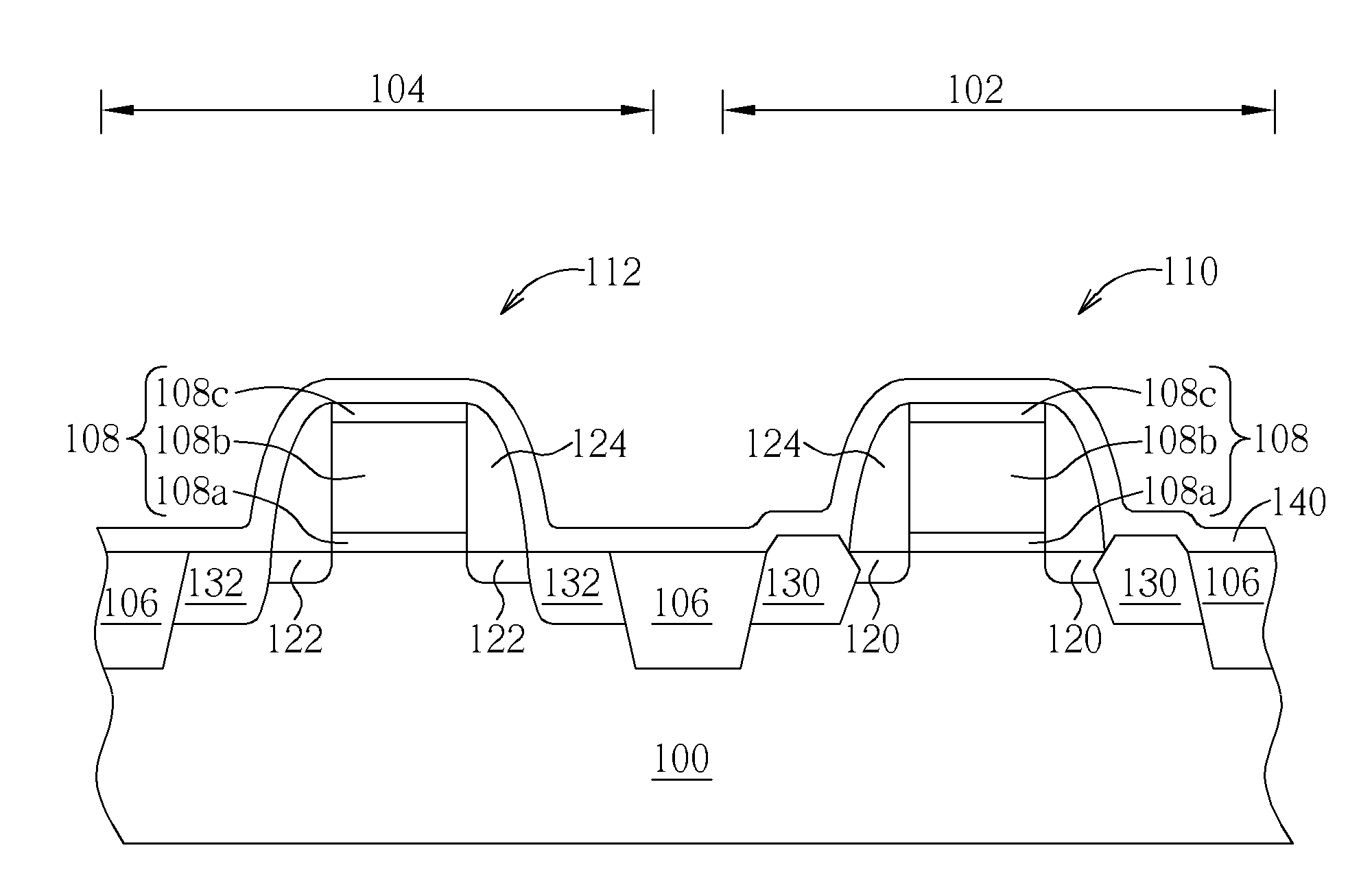
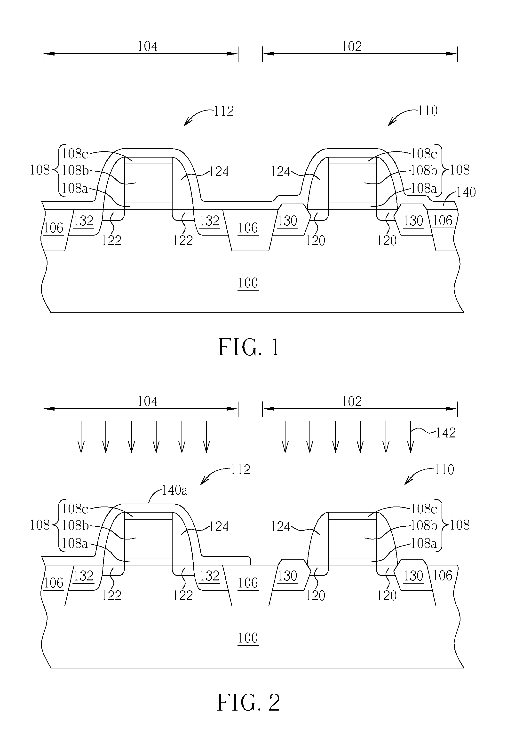
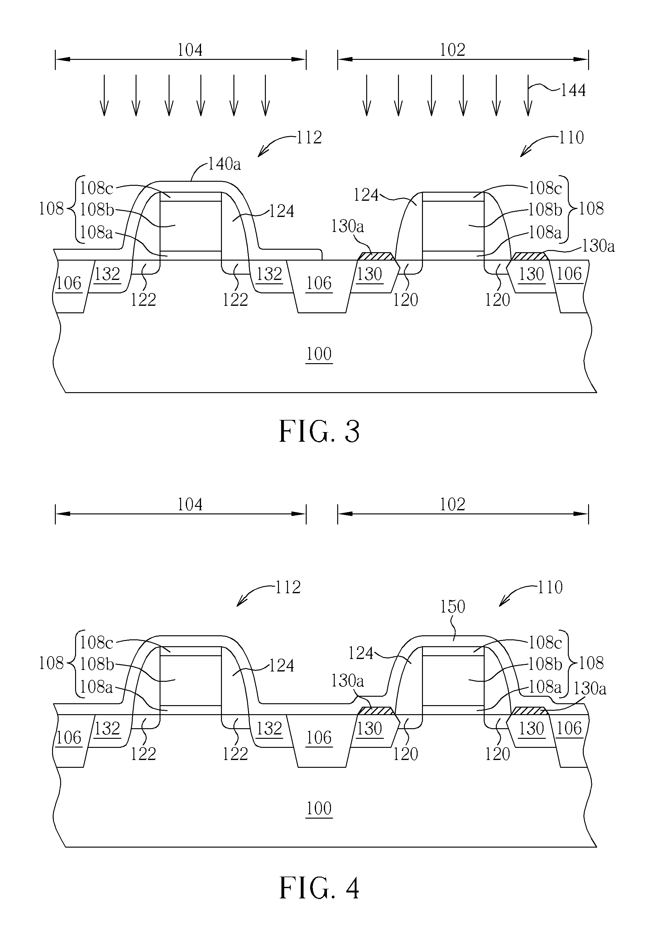
[0016]Please refer to FIGS. 1-6, which are schematic drawings illustrating a method for manufacturing a semiconductor device provided by a preferred embodiment of the present invention. As shown in FIG. 1, the preferred embodiment first provides a substrate 100 having a first region 102 and a second region 104 defined thereon. A first transistor device 110 and a second transistor device 112 are respectively formed in the first region 102 and the second region 104. And a plurality of shallow trench isolations (STIs) 106 providing electrical isolation is formed between the first transistor device 110 and the second transistor device 112 in the substrate 100. The first transistor device 110 includes a first conductivity type and the second transistor device 112 includes a second conductivity type. In the preferred embodiment, the first conductivity type and the second conductivity type are complementary. For example, the first transistor device 110 is a p-type transistor device while t...
PUM
 Abstract
Description
Claims
Application Information