
E-mode hfet device

Active Publication Date: 2013-06-27
QUALCOMM INC
View PDF11 Cites 57 Cited by
  • Summary
  • Abstract
  • Description
  • Claims
  • Application Information

AI Technical Summary

Benefits of technology

The present invention introduces a new transistor design that utilizes a special semiconductor structure called a Hetero junction FET. This design replaces the traditional metal gate with a stack comprising a highly doped compound semiconductor and an insulating layer. This results in enhanced performance and reduced gate current leakage. The insulating layer and highly doped semiconductor allow for easy tuning of the device's threshold voltage, making it highly flexible. The invention can be manufactured using both polar and non-polar materials. Furthermore, a back-barrier layer and heavily doped threshold tuning layer are used to suppress Short Channel Effect phenomena and adjust the device's threshold voltage.

Problems solved by technology

However the need to further improve its general performance while reducing its cost is still a necessity that poses a significant challenge.
However, the reduction of Lg alone does not lead to maximum RF performance.
Another important limitation of these structures is the difficulty to make them operate in enhancement mode.
The enhancement behavior of the previous structure has also another disadvantage: in order to isolate the source and the drain terminals from the gate, the gate region must be made smaller than the etched region formed in the barrier layer, leaving two isolating regions 9 and 7 at the sides of the gate.
This causes a discontinuity in the doping modulation of the channel, adding two extra resistive paths in the channel.
HEMT employing polar materials such as GaN and III-Nitride alloys oriented along the direction, present similar limitations.
This is due to the lack of stable metal alloys with high work-function to be used as gate electrode.
This solution therefore degrades the carrier confinement in the GaN channel layer and is very susceptible to process variations.
The solution proposed by Ueno et al., even if very efficient in order to obtain an enhancement mode GaN device, still does not solve the problem associated with the parasitic gate diode that can turn on at moderate low positive gate voltages limiting the electron enhancement in the channel portion under the gate.
However, if holes are injected into the channel, their recombination time limits the switching speed of the device deteriorating the overall device performance.
Furthermore, in general p-type dopant in compound semiconductor are not easy to deal with respect to n-type ones.
Although the cited prior art references describe structures that offer some of the described advantages, no one device includes all of them, limiting their ability to solve the problem of obtaining transistors with high RF performance, low power dissipation and low on-resistance per given semiconductor area in integrated circuits.

Method used


Image

  • E-mode hfet device
  • E-mode hfet device
  • E-mode hfet device

Examples


Embodiment Construction

A FIG. 4

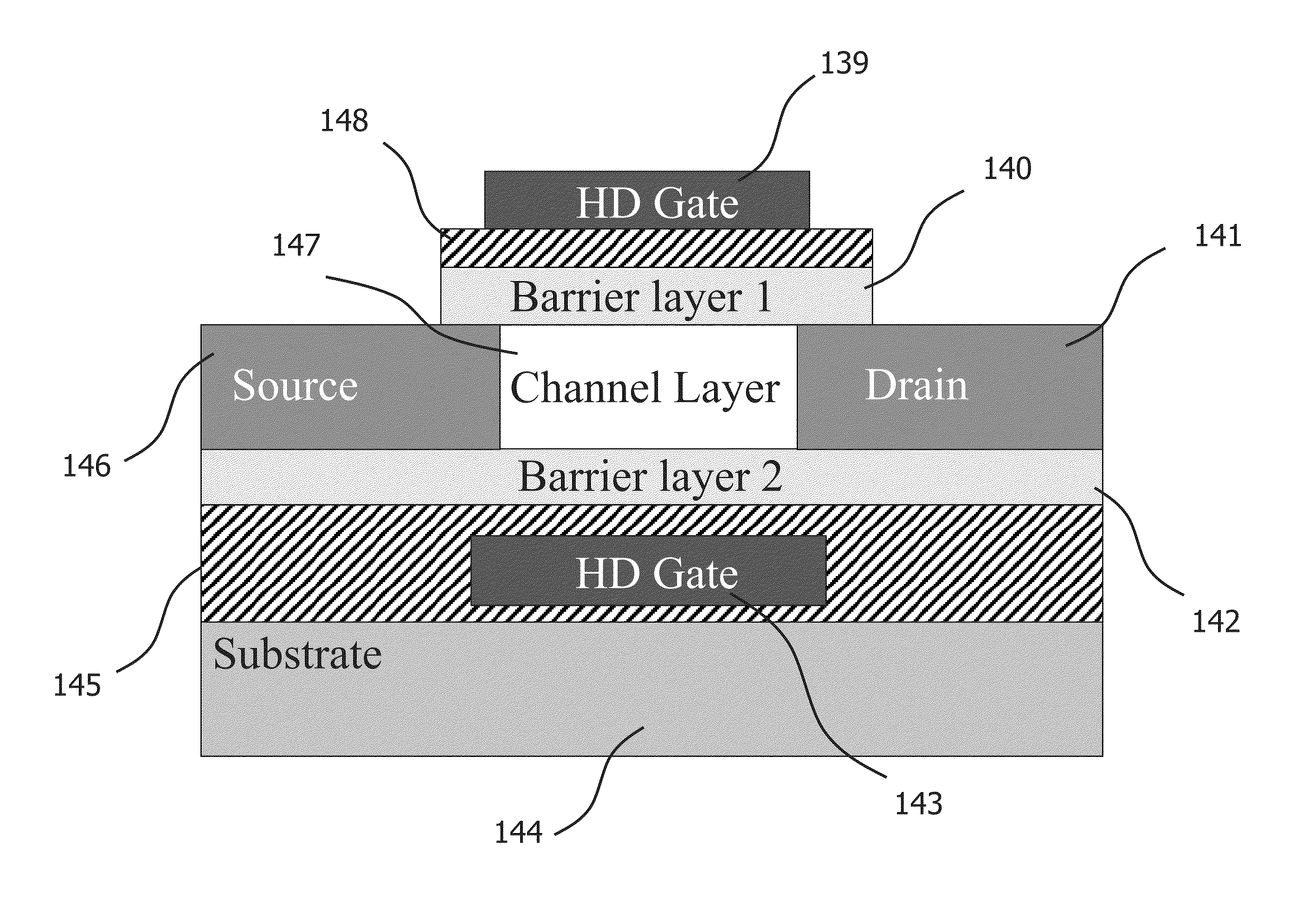
[0077]FIG. 4 is showing a Hetero-structure FET (HFET) device according to the preferred embodiment of the invention. The metallic or n+-type semiconductor regions 28 and 25 define the source and the drain of the transistor. Regions 29 corresponds to the barrier layer of the device, and the channel layer 27 is the region where the electron (or hole)—channel is formed. Region 23, which is formed by a heavily doped semiconductor layer on the top of an insulating layer 24, corresponds to the gate of the device.

[0078]If the desired device is an n-channel HFET, the channel region should have an electron affinity greater with respect to the barrier layer 29, in order to confine the carrier transport inside the layer 27 during the normal operation of the device. The gate region 23 instead, can be built with the same, greater or lower electron affinity with respect to the barrier layers, depending on the desired device characteristics. If necessary, the gate 23 and / or the barrier lay...


PUM


Abstract

The present invention describes a transistor based on a Hetero junction FET structure, where the metal gate has been replaced by a stack formed by a highly doped compound semiconductor and an insulating layer in order to achieve enhancement mode operation and at the same time drastically reduce the gate current leakage. The combination of the insulating layer with a highly doped semiconductor allows the tuning of the threshold voltage of the device at the desired value by simply changing the composition of the semiconductor layer forming the gate region and / or its doping allowing a higher degree of freedom. In one of the embodiment, a back-barrier layer and a heavily doped threshold tuning layer are used to suppress Short Channel Effect phenomena and to adjust the threshold voltage of the device at the desired value. The present invention can be realized both with polar and non-polar (or semi-polar) materials.

Description

BACKGROUND OF THE INVENTION[0001]1. Field of the Invention[0002]The present invention is in the field of semiconductor structures. The present invention is further in the field of semiconductor structures of transistor devices. The present invention further relates to the field of integrated devices and circuits. The implementation is not limited to a specific technology, and applies to either the invention as an individual component or to inclusion of the present invention within larger systems which may be combined into larger integrated circuits.[0003]2. Brief Description of Related Art[0004]The semiconductor transistor is the most important component for large integrated circuits. In the last three decades, field effect transistors (FETs) used in current integrated circuit process technologies have undergone a continuous shrinking of the semiconductor area needed for elementary components, and new materials including III-V and II-VI semiconductor compounds have been introduced t...

Claims


Application Information

Patent Timeline
IPC IPC(8): H01L29/778H01L21/336
CPCH01L29/42316H01L29/42364H01L29/42372H01L29/1075H01L29/7787H01L29/1029H01L29/7782
Inventor MARINO, FABIO ALESSIOMENEGOLI, PAOLO
Owner QUALCOMM INC
Learn More