

Spectrometry device and spectrometry method
a spectrometry device and spectrometry technology, applied in the direction of optical radiation measurement, fluorescence/phosphorescence, instruments, etc., can solve the problem of difficult downsizing of the apparatus, and achieve the effect of performing highly accurate measurement with eas
- Summary
- Abstract
- Description
- Claims
- Application Information
AI Technical Summary
Benefits of technology
Problems solved by technology
Method used
Image

Examples
first exemplary embodiment
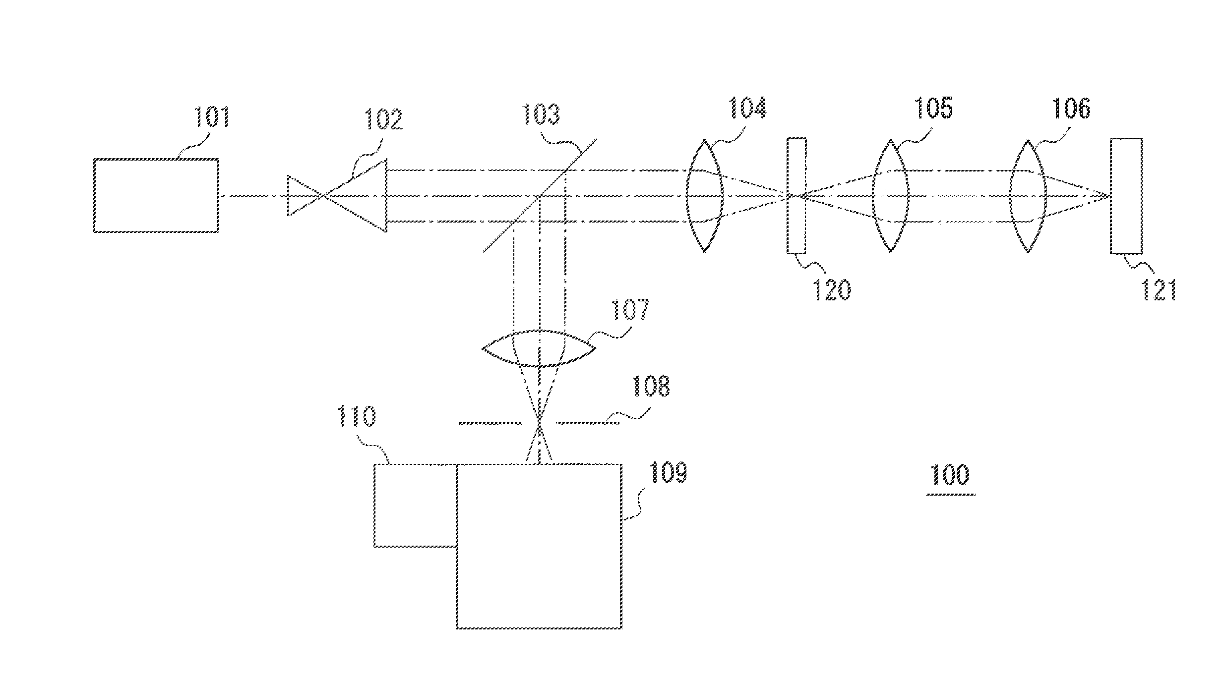
[0040]Exemplary embodiments according to the present invention are explained hereinafter with reference to the drawings. Firstly, an overall configuration of a spectrometry device according to this exemplary embodiment is explained with reference to FIG. 1, FIG. 1 shows a spectrometry device. A spectrometry device according to this exemplary embodiment is a Raman spectrometry device that disperses Raman scattered light generated in a sample and thereby measures the Raman scattered light.
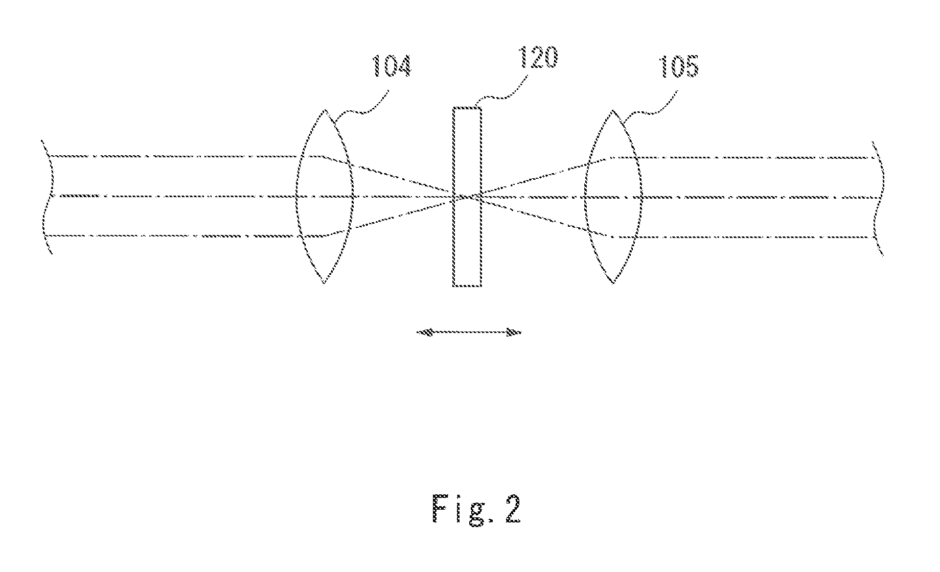
[0041]As shown in FIG. 1, a spectrometry device 100 includes a laser light source 101, a beam expander 102, a beam splitter 103, a lens 104, a lens 105, an objective lens 106, a lens 107, an entrance slit 108, a spectroscope 109, and a detector 110. The spectrometry device 100 is a Raman microscope that detects Raman scattered light, and includes the spectroscope 109 for performing spectrometry. Further, Raman spectrometry is performed by simultaneously irradiating a reference sample 120 and a measur...
second exemplary embodiment
[0065]A spectrometry device according to this exemplary embodiment is explained with reference to FIG. 3. FIG. 3 shows a configuration of a spectrometry device 100. In this exemplary embodiment, an optical scan system using a galvano-mirror is added to the optical system of the spectrometry device shown in the first exemplary embodiment. Therefore, in FIG. 3, a mirror 131 and a galvano-mirror 132 are added in the spectrometry device 100 shown in FIG. 1. Note that explanation of the components / configurations that are the same as those of the first exemplary embodiment is omitted as appropriate.
[0066]The mirror 131 and the galvano-mirror 132 are disposed between the beam splitter 103 and the lens 104. Therefore, the laser light that has passed through the beam splitter 103 is reflected on the mirror 131 and is incident on the galvano-mirror 132. Since the galvano-mirror 132 deflects the laser light, the incident position of the laser light on the measurement sample 121 is changed. Tha...
third exemplary embodiment
[0074]A spectrometry device according to this exemplary embodiment is explained with reference to FIG. 5. In this exemplary embodiment, a reference sample 26 is disposed in the optical system shown in FIG. 7 of Patent literature 1. Note that explanation of the components / configurations that are the same as those of the first or second exemplary embodiment and the components / configurations that are the same as those of Patent literature 1 is omitted as appropriate.
[0075]A spectrometry device 100 includes, as a configuration for observing a measurement sample 22, a laser light source 10, a beam expander 11, a Y-scan device 13, a lens 14, an iris 15, a lens 16, a beam splitter 17, an X-scan mirror 18, a lens 19, a lens 20, an objective lens 21, a stage 23, a lens 24, an spectroscope 31, a detector 32, a stage drive device 40, and a processing device 50. Further, the spectroscope 31 includes an entrance slit 30 on the incident side. The reference sample 26 is disposed between the lens 1...
PUM
 Abstract
Description
Claims
Application Information