Photovoltaic cell assembly and method

Inactive Publication Date: 2013-07-04
DOW GLOBAL TECH LLC
View PDF13 Cites 17 Cited by
  • Summary
  • Abstract
  • Description
  • Claims
  • Application Information

AI Technical Summary

Benefits of technology

[0022]FIG. 11 is a graphical example of the effect of wire resistivity on the ser

Problems solved by technology

The elimination of conductive adhesive may be desirous, because conductive adhesiv

Method used


Image

  • Photovoltaic cell assembly and method
  • Photovoltaic cell assembly and method
  • Photovoltaic cell assembly and method

Examples


examples

[0054]In the following paragraphs, five (5) examples of the present invention and one (1) comparative example are presented. The following examples are provided to illustrate the invention but are not intended to limit the scope thereof.

examples generally

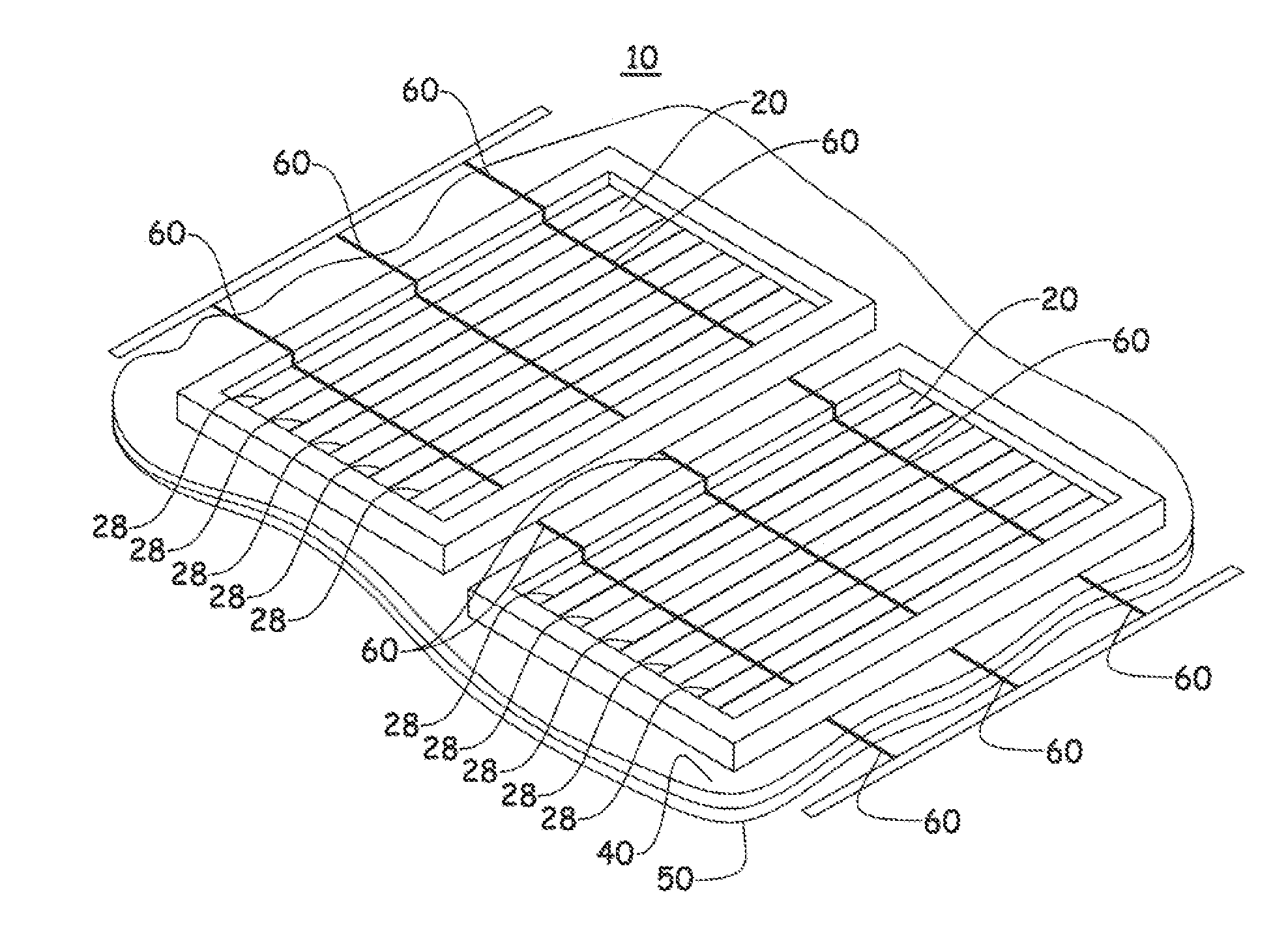
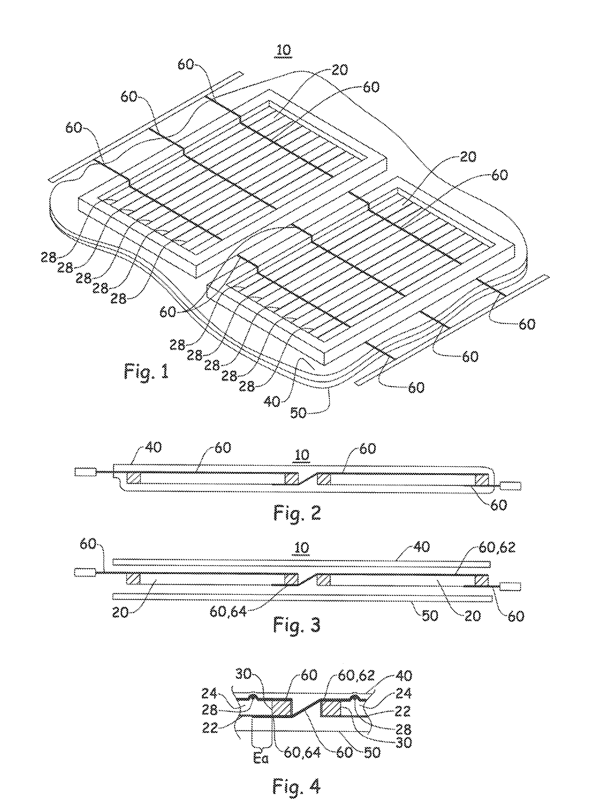
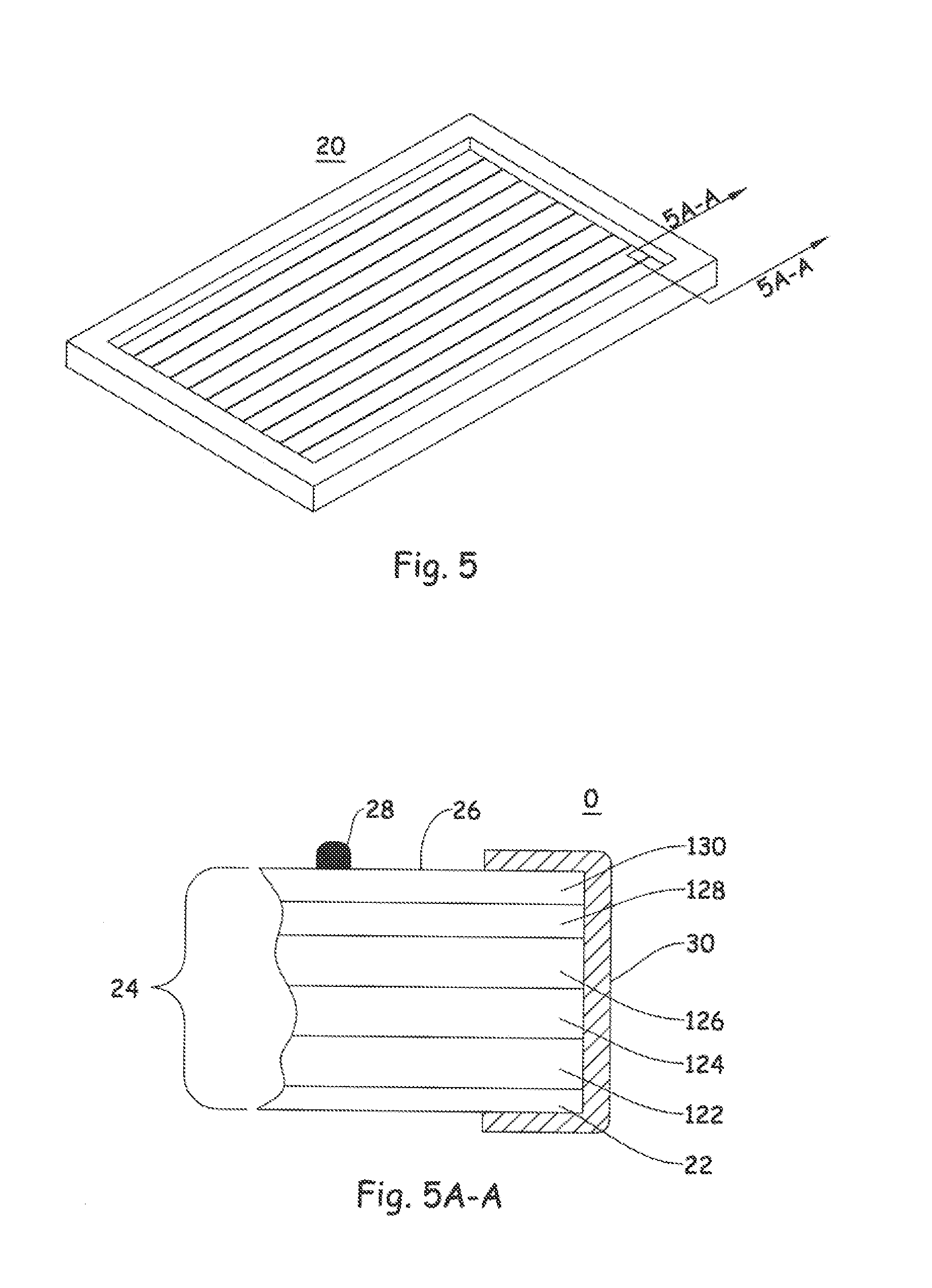
[0055]For the purpose of these examples, CIGS type solar cells (50 mm×210 mm), on stainless steel substrate (e.g. conductive substrate layer 22), are obtained from Global Solar Inc. The cells are cut into smaller cells 50 mm (“L”)×25 mm (“W”). A Ni / Ag grid (e.g. collection structure 28) is applied to the top surface 26 of the cell onto the transparent conductive layer (ITO). In this case thirty (30) lines spanning across the larger cell dimension. The cells 20 are scribed down to the Mo layer (122) near the edge of the cells (e.g. from the outer edge, inboard about 1.0 to 2.0 mm). It is believed that use of such scribing is common in industry because of damage due from cutting the cell 20.

[0056]The symbols and short-hand notations herein are defined as:

[0057]VCC=voltage−open circuit

[0058]ISC=current−short circuit

[0059]FF=fill factor

[0060]Eff=efficiency

[0061]RS=series resistance

[0062]Rsh=shunt (parallel) resistance

[0063]RP=Rsh

[0064]Pmax−Power (watts)

[0065]JSC=current−short circuit p...

example 1

[0066]Two cells with the grids shown in FIG. 7 were treated on all four edges with polyimide (“kapton”®) tape (e.g. non-conductive layer portion 30) in such a manner that it was wrapped around the edge and covered the scribe section on the top of the cell. Three pieces of Ag-coated wire (30 AWG; e.g. conductive elements 60) was then applied to the surface of cell A and extended to the bottom of cell B, where the ends were attached locally to the stainless steel substrate using kapton tape (prior to the application of the encapsulants 40, 50). In a similar fashion, three pieces of 30 AWG Sn-coated wire were applied to the surface of cell A and extended beyond the cell edge. The wires were applied in a direction perpendicular to the direction of the fingers of the silver grid. No bonding material was used to attach the wire to the surface of the cells, (although a small piece of tape may be used to hold the elements 60 in-place until the lamination process can occur). The two cell ass...


PUM


Abstract

The present invention provides an improved photovoltaic cell assembly (10) that includes at least plurality of photovoltaic calls (20). The cells include a photoactive portion (24) sandwiched between a top electrically conductive structure (28) on some regions of a top surface (28) of the photoactive portion leaving exposed top surface on other regions; and an opposing conductive substrate layer (22). The improved photovoltaic cell assembly also includes a plurality of conductive elements (80); a first encapsulant layer (40) In contact with the top electrically conductive structure and the exposed fop surface of the photoactive portion; and a second encapsulant layer (50) in contact with the opposing conductive substrate layer, the encapsulants holding the conductive elements to the cell layers.

Description

CLAIM OF PRIORITY[0001]The present application claims the benefit of the filing date of U.S. Provisional Application No. 61 / 383,867 (filed 17-Sep.-2010) the contents of which are hereby incorporated by reference in their entirety.FIELD OF THE INVENTION[0002]The present invention relates to an improved photovoltaic (PV) cell assembly, more particularly to an improved photovoltaic cell assembly that interconnects a plurality of cells without solder or conductive adhesive.BACKGROUND[0003]Photovoltaic articles often comprise a number of electrically interconnected photovoltaic cells. In addition to ensuring electrical interconnection, these cells are sometimes packaged to protect the cells from damage from handling or the environment. The conventional approach to electrical interconnection of photovoltaic cells is the so-called string & tab method, in which solar cells are connected to each other using tin or solder coated flat wire (bus) ribbons and bonded by soldering and / or other adh...

Claims


Application Information

Patent Timeline
IPC IPC(8): H01L31/05
CPCH01L31/048H01L31/0504Y02E10/541H01L31/0749H01L31/0481
Inventor DEGROOT, MARTY W.MILLS, MICHAEL E.PARSONS, THOMAS J.RAMESH, NARAYANSTEMPKI, MATTWIRSING, DOUGLAS J.
Owner DOW GLOBAL TECH LLC
Why Eureka
Try Eureka