Y-branch dual optical phase modulator

a dual optical phase, y-branch technology, applied in non-linear optics, instruments, optics, etc., can solve the problems of non-flat step response, unstable eo characteristic of ape waveguide exposed to vacuum, etc., to reduce the non-uniformity of electrical resistivity of the substrate lateral

Inactive Publication Date: 2013-07-04
JDS UNIPHASE CORP
View PDF6 Cites 19 Cited by
  • Summary
  • Abstract
  • Description
  • Claims
  • Application Information

AI Technical Summary

Benefits of technology

[0012]One aspect of the present invention provides a Y-branch DOPM, comprising: a substrate comprising electro-optical material; first, second and third optical ports formed in or upon the substrate for coupling light in and out of the substrate; and a Y-branch waveguide structure (YBWS) formed in the substrate for optically connecting the first optical port with each of the second and third optical ports, the YBWS comprising: a first waveguide arm coupled to the first port, a second waveguide arm coupled to the second port and having a modulating waveguide segment, a third waveguide coupled to the third port and having a modulating waveguide segment, and an optical splitter optically connecting the first waveguide arm to each of the first and second waveguide arms. A co-planar electrode system is provided comprising two signal electrodes and at least one ground electrode disposed upon the substrate alongside the modulating waveguide segments of the second and third waveguide arms so that each of the modulating waveguide segments is located in an electrode gap separating one of the signal electrodes and the at least one ground electrode for inducing an electric field in the first and second modulating waveguide segments when a voltage is applied between the signal and ground electrodes. Each of the modulating waveguide segments gradually widens by at least 20% towards a middle portion thereof over a length of at least 50 μm for reducing a lateral non-uniformity of electrical resistivity of the substrate across the electrode gaps.

Problems solved by technology

It was found, however, that electro-optic (EO) characteristic of APE waveguides may be unstable when exposed to vacuum.
However, although the use of Ti waveguides in the modulation portion of YBDPM 10 as described by Feth does appear to improve the device performance, we found that the electro-optic (EO) response of YBDPM 10 still suffers from non-idealities resulting in a non-flat step response, when the optical phase shift in the waveguide continues to change for minutes after a step-wise change in an applied voltage to an new dc level, and a non-flat frequency response of electro-optic characteristics at frequencies below 1 Hz.

Method used


Image

  • Y-branch dual optical phase modulator
  • Y-branch dual optical phase modulator
  • Y-branch dual optical phase modulator

Examples


Embodiment Construction

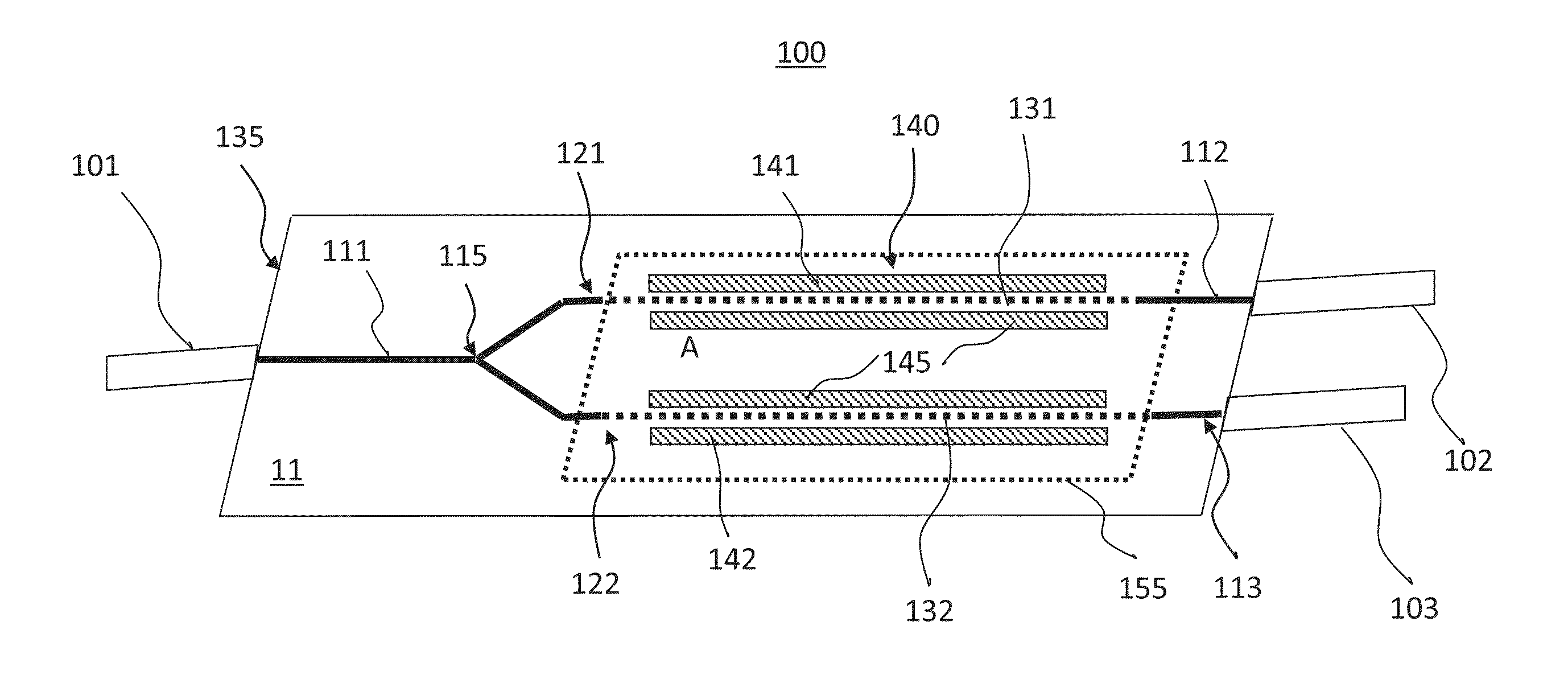
[0050]In the context of this specification, the terms ‘disposed on / upon’, ‘located on / upon’ and their equivalents are used to indicate relative position of two elements and encompass situations wherein two elements are in a direct physical contact or have one or more additional elements between them. The term “disposed directly on / upon” means herein that the two elements are in a direct physical contact. The term ‘low frequency’ with reference to an EO frequency response or modulation efficiency means herein frequencies from about 1 Hz down to 0.00001 Hz or less, unless stated otherwise. The term ‘low-frequency application’ is used herein to mean applications wherein the device is modulated at frequencies generally below about 1 MHz and including frequencies in the range from about 1 Hz down to 0.00001 Hz or less, unless stated otherwise.

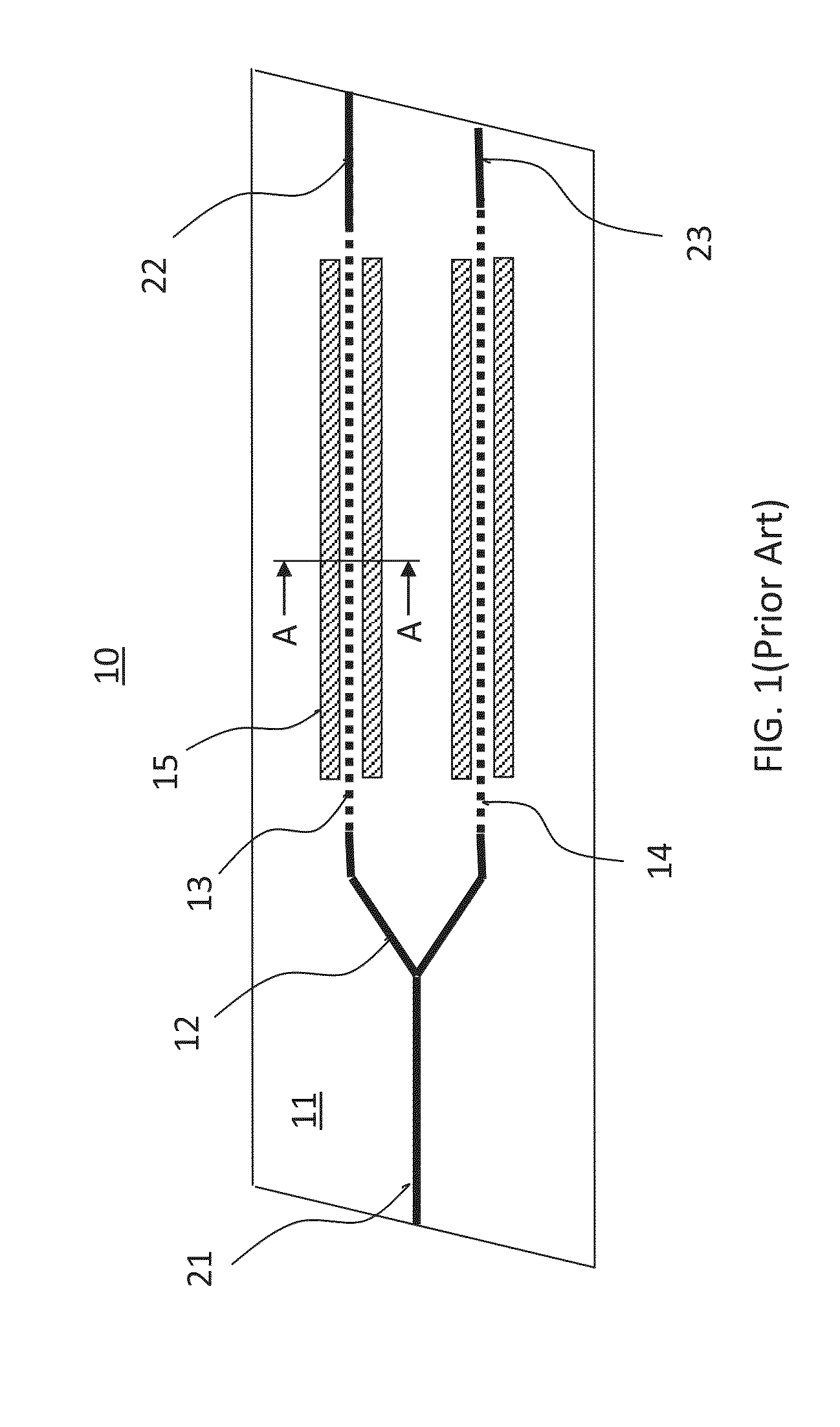
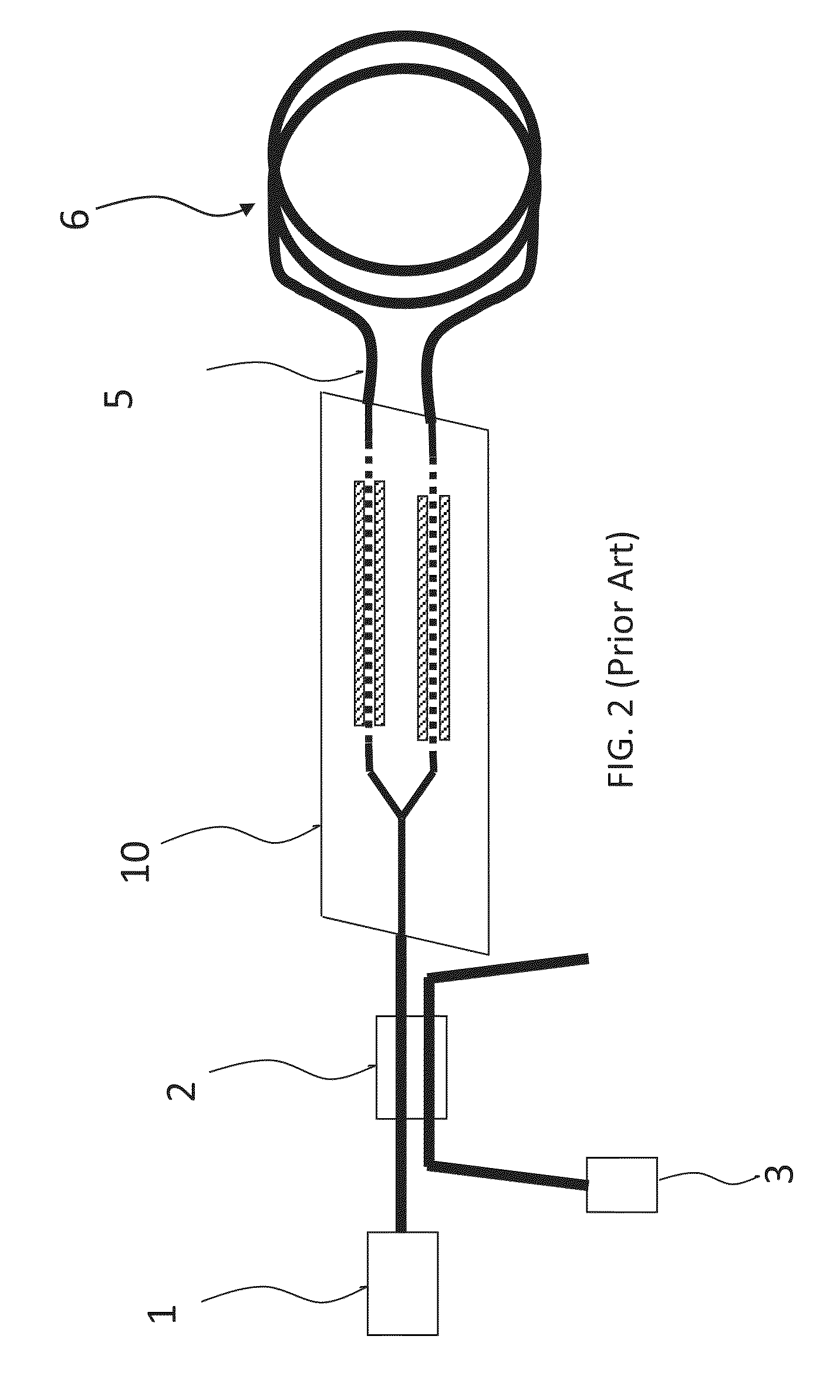
[0051]Prior to providing a detailed description of exemplary embodiments, we first describe some drawbacks of prior art YBDPM devices, in particula...


PUM

PropertyMeasurementUnit
modulation frequenciesaaaaaaaaaa
distanceaaaaaaaaaa
widthaaaaaaaaaa

Abstract

The invention relates to Y-branch waveguide dual optical phase modulators with improved electro-optic (EO) frequency and step responses at frequencies below 1 Hz for use in low-frequency applications such fiber-optic gyroscopes. A Y-branch waveguide structure is formed in an EO substrate, with three or more electrodes used to form a waveguide phase modulator in each of two output waveguide arms. In one embodiment an insulating buffer layer is provided between at least a portion of the electrodes and the substrate for flattening the low-frequency EO response by reducing the modulation efficiency below 1 Hz. In one embodiment each of the waveguide phase modulators includes two ground electrodes extending along both sides of a signal electrode. A top portion of the substrate may be doped to reduce lateral variations of the substrate conductivity in the waveguide and non-waveguide portions thereof between corresponding signal and ground electrodes.

Description

TECHNICAL FIELD[0001]The present invention generally relates to electrooptic waveguide modulators, and more particularly relates to electrooptic two-output Y-branch waveguide modulators with a flattened time-domain step response and a flattened low-frequency response.BACKGROUND OF THE INVENTION[0002]Optical modulators that are based on electro-optical materials incorporating voltage-controlled waveguides are well known in the art and are used in a variety of applications. For high bandwidth application, for example at modulation rates in the 5 GHz to 40 GHz range, such modulators typically include waveguides forming a Mach-Zehnder interferometer structure to achieve optical intensity modulation at the optical output of the device; such modulators are conventionally referred to as Mach-Zehnder (MZ) modulators. High-speed MZ modulators utilize travelling-wave radio-frequency (RF) electrode systems and are described, for example, in an article by E. L. Wooten et al, entitled “A Review ...

Claims


Application Information

Patent Timeline
Patent Type & Authority Applications(United States)
IPC IPC(8): G02F1/035
CPCG02F1/035G02F2201/07G02F1/0316
Inventor KISSA, KARLXU, JASON JIAZHAN
Owner JDS UNIPHASE CORP
Why Eureka
Try Eureka