Semiconductor device and method for manufacturing same

a technology of semiconductors and semiconductors, applied in the direction of semiconductor devices, basic electric elements, electrical appliances, etc., can solve the problems of disadvantageous degradation of breakdown voltage characteristics and reduced resistance, and achieve the effect of improving breakdown voltage characteristics and reducing resistan

Active Publication Date: 2013-07-18
SUMITOMO ELECTRIC IND LTD
View PDF4 Cites 12 Cited by
  • Summary
  • Abstract
  • Description
  • Claims
  • Application Information

AI Technical Summary

Benefits of technology

[0008]The present invention has been made in view of the foregoing problem, and one object of the present invention is to provide a semiconductor device having improved breakdown voltage characteristics and reduced ON resistance, as well as a method for manufacturing such a semiconductor device.

Problems solved by technology

In the trench gate type MOSFET, ON resistance can be reduced, but breakdown voltage characteristics are disadvantageously deteriorated due to electric field concentration on a gate insulating film formed in a bottom portion of the trench.

Method used


Image

  • Semiconductor device and method for manufacturing same
  • Semiconductor device and method for manufacturing same
  • Semiconductor device and method for manufacturing same

Examples


embodiment 1

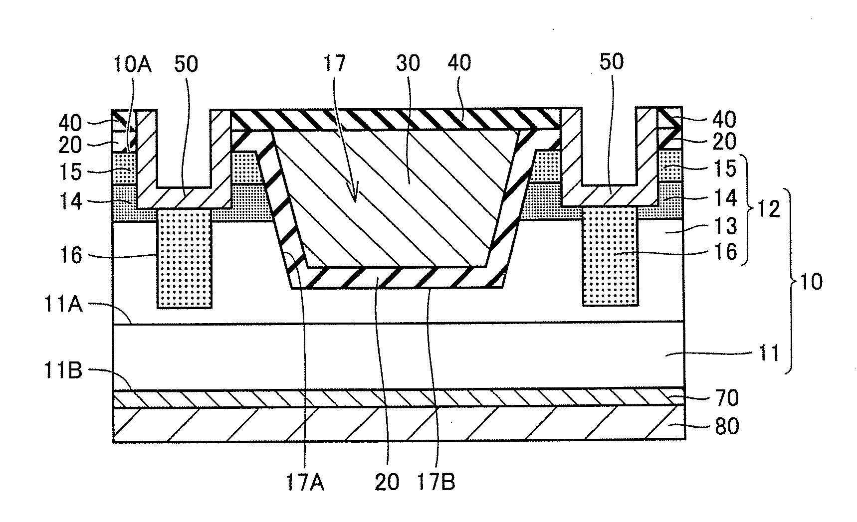
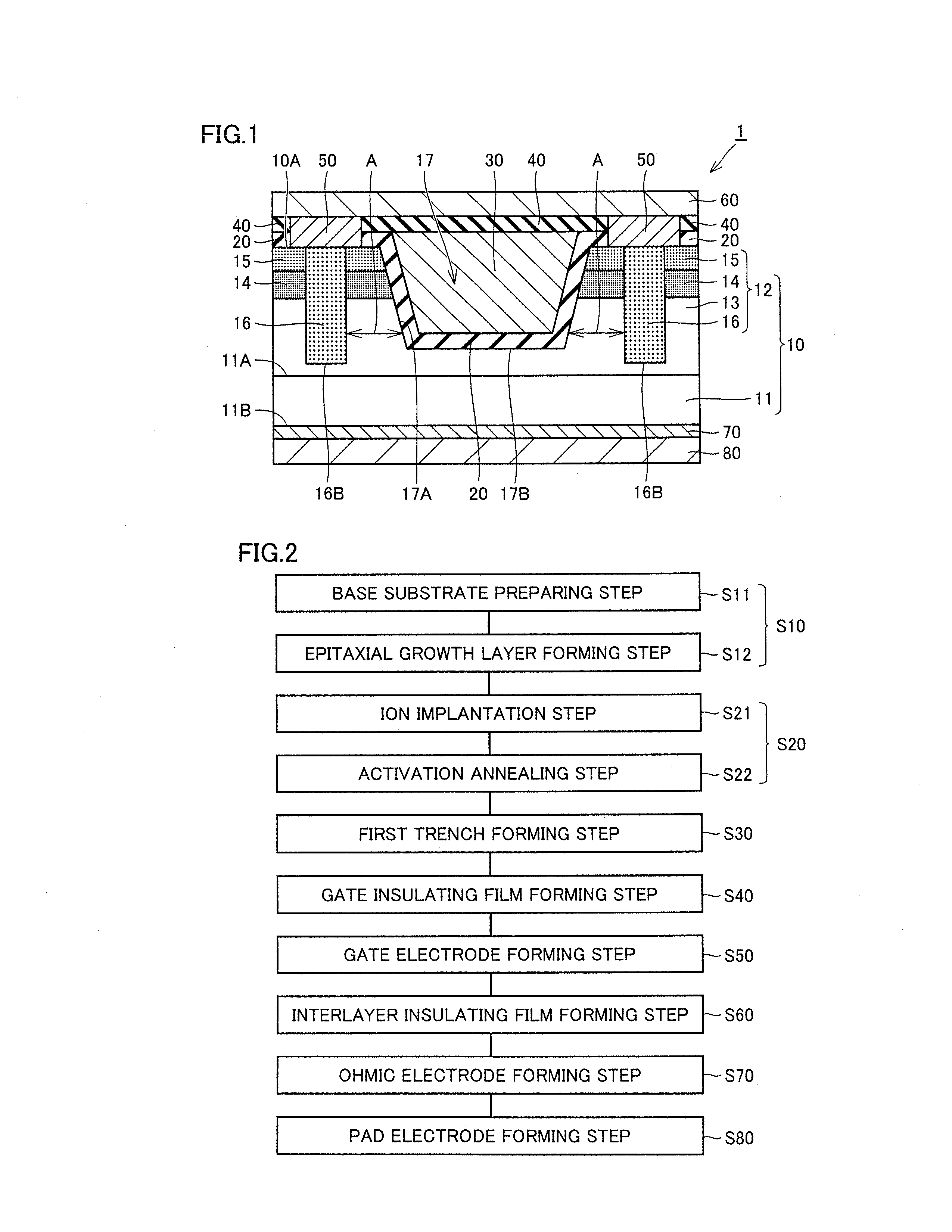
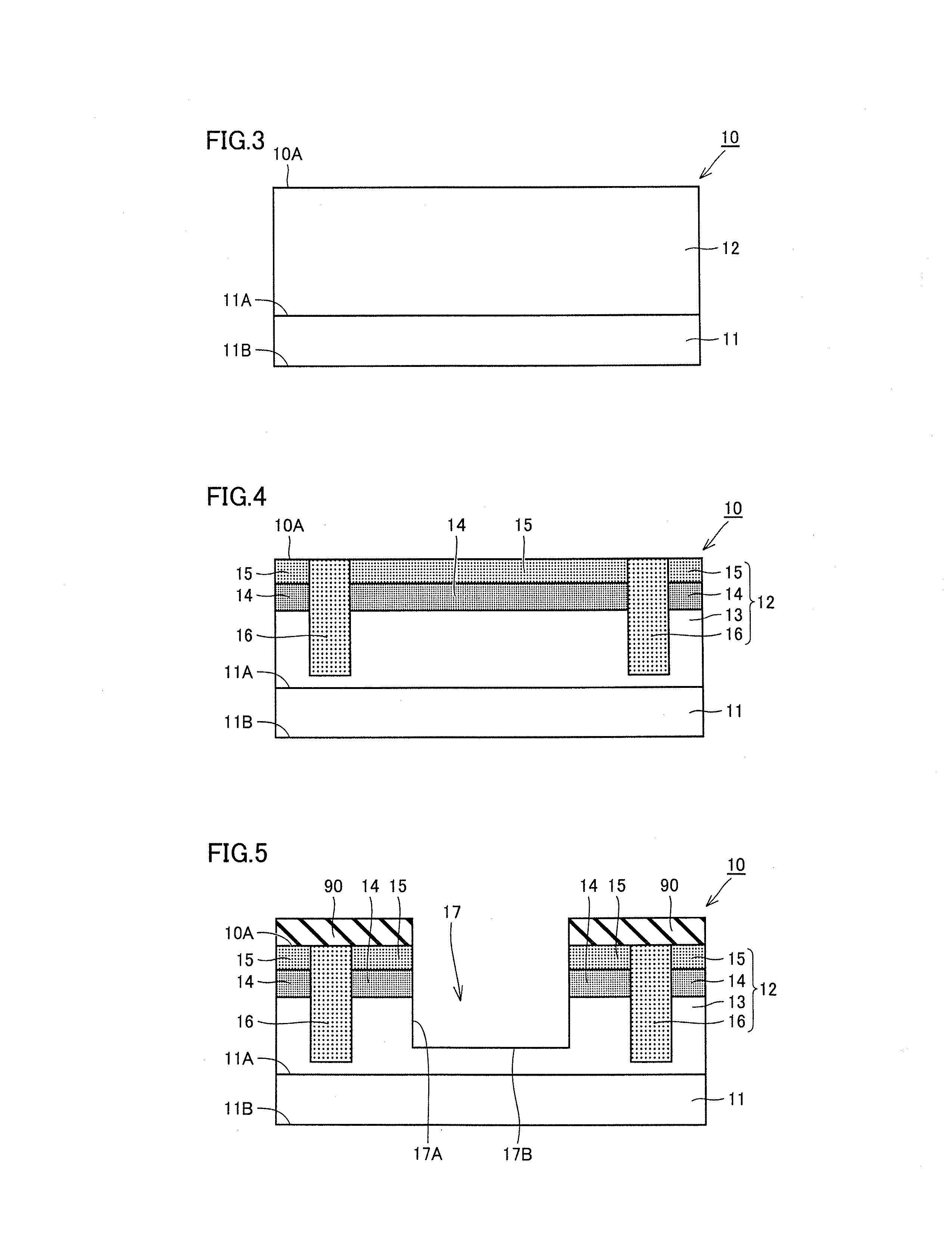
[0045]Embodiment 1 as one embodiment of the present invention will now be described. First, a structure of a MOSFET 1 serving as a semiconductor device in accordance with the present embodiment will be described. Referring to FIG. 1, MOSFET 1 includes a substrate 10 made of silicon carbide and having a main surface 10A, a gate insulating film 20, a gate electrode 30, an interlayer insulating film 40, a source electrode 50, a source pad electrode 60, a drain electrode 70, and a drain pad electrode 80. Substrate 10 includes a base substrate 11 and a semiconductor layer 12. In semiconductor layer 12, a drift region 13, a body region 14, a source region 15, and a deep region 16 are formed. Substrate 10 has a first trench 17 formed therein, first trench 17 opening on a main surface 10A side and having wall surfaces 17A and a bottom surface 17B.

[0046]Base substrate 11 is made of silicon carbide, contains an n type impurity such as N (nitrogen), and therefore has n type conductivity (a fir...

embodiment 2

[0077]Next, Embodiment 2 as another embodiment of the present invention will be described. First, a structure of a MOSFET 2 serving as a semiconductor device in accordance with the present embodiment will be described. Referring to FIG. 10, MOSFET 2 basically has the same structure, operates in the same manner, and exhibits the same effect as those of MOSFET 1 in Embodiment 1. However, MOSFET 2 is different from MOSFET 1 in that, as shown in FIG. 10, a second trench 18 different from first trench 17 is formed in substrate 10, and source electrode 50 serving as a contact electrode is disposed on and in contact with wall surfaces 18A and a bottom surface 18B of second trench 18.

[0078]Referring to FIG. 10, second trench 18 opens on the main surface 10A side, and has wall surfaces 18A and bottom surface 18B. Specifically, second trench 18 is formed to penetrate source region 15 and reach body region 14, that is, to be shallower than first trench 17.

[0079]Source electrode 50 is disposed ...


PUM


Abstract

A MOSFET includes: a substrate having a first trench formed therein, the first trench opening on a side of one main surface; a gate insulating film; and a gate electrode. The substrate includes an n type source region, a p type body region, an n type drift region, and a p type deep region making contact with the body region and extending to a region deeper than the first trench. The first trench is formed such that a distance between the wall surface and the deep region increases with increasing distance from the main surface of the substrate.

Description

BACKGROUND OF THE INVENTION[0001]1. Field of the Invention[0002]The present invention relates to a semiconductor device and a method for manufacturing the same, and more particularly to a semiconductor device having improved breakdown voltage characteristics and reduced ON resistance, as well as a method for manufacturing such a semiconductor device.[0003]2. Description of the Background Art[0004]In recent years, in order to achieve a high breakdown voltage, low loss, and the like of semiconductor devices, silicon carbide has been adopted as a material for semiconductor devices. Silicon carbide is a wide band gap semiconductor having a band gap larger than that of silicon, which has been conventionally widely used as a material for semiconductor devices. Hence, by adopting silicon carbide as a material for a semiconductor device, the semiconductor device can have a high breakdown voltage, reduced ON resistance, and the like.[0005]An exemplary semiconductor device adopting silicon ca...

Claims


Application Information

Patent Timeline
Patent Type & Authority Applications(United States)
IPC IPC(8): H01L29/78H01L29/66
CPCH01L29/6606H01L29/7827H01L21/0475H01L21/0485H01L29/41766H01L29/4236H01L21/3065H01L29/66068H01L29/7813H01L29/045H01L29/1095H01L29/1608H01L29/45
Inventor MASUDA, TAKEYOSHIWADA, KEIJIHIYOSHI, TORU
Owner SUMITOMO ELECTRIC IND LTD
Why Eureka
Try Eureka