Processing method for wafer

a processing method and wafer technology, applied in the field of processing methods of wafers, can solve problems such as optical device wafers sometimes broken

Active Publication Date: 2013-07-25
DISCO CORP
View PDF6 Cites 59 Cited by
  • Summary
  • Abstract
  • Description
  • Claims
  • Application Information

AI Technical Summary

Benefits of technology

[0009]Therefore, it is an object of the present invention to provide a processing method for a wafer wherein the wafer is not broken along a modified layer when the wafer is taken out from a laser processing apparatus and transported to a next stage and has a reflecting film on the rear face thereof.

Problems solved by technology

However, the dividing method for a sapphire wafer just described has a problem in that, in the middle of a procedure wherein an optical device wafer in which a modified layer is formed is taken out from a laser processing apparatus and transported to a reflecting film forming apparatus for forming a reflecting film on the rear face of the optical device wafer or when such optical device wafer is taken out from the laser processing apparatus, the optical device wafer is sometimes broken.

Method used


Image

  • Processing method for wafer
  • Processing method for wafer
  • Processing method for wafer

Examples


Embodiment Construction

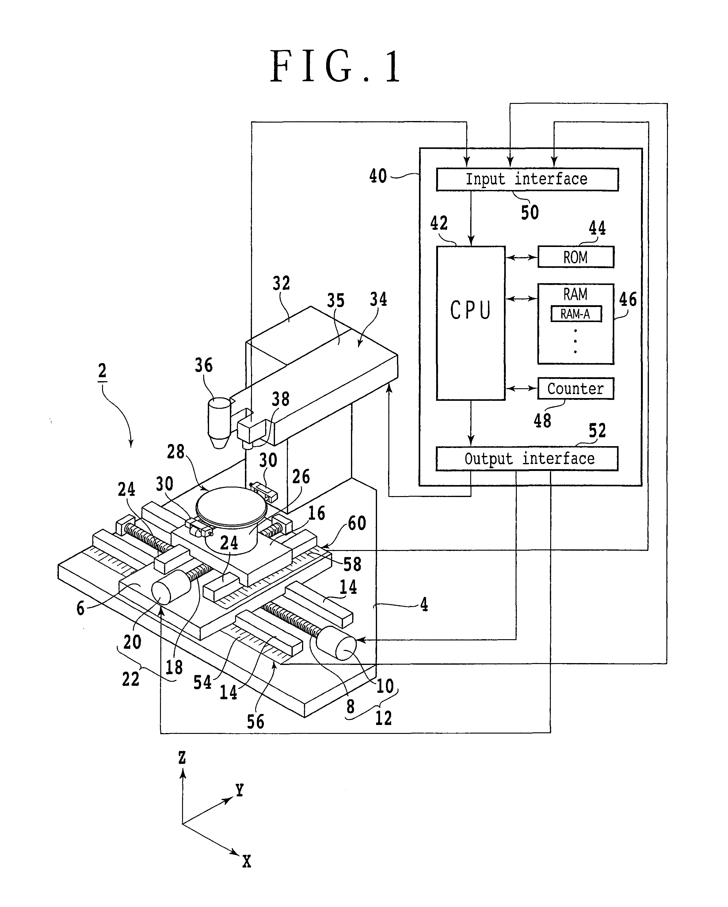
[0026]In the following, an embodiment of the present invention is described in detail with reference to the drawings. FIG. 1 shows a schematic block diagram of a laser processing apparatus 2 suitable for carrying out a modified layer forming step in a wafer processing method of the present invention. The laser processing apparatus 2 includes a first slide block 6 mounted for movement in an X-axis direction on a stationary base 4. The first slide block 6 is moved in a processing feeding direction, that is, in the X-axis direction, along a pair of guide rails 14 by processing feeding means 12 configured from a ball screw 8 and a step motor 10.

[0027]A second slide block 16 is mounted for movement in a Y-axis direction on the first slide block 6. In particular, the second slide block 16 is moved in an indexing direction, that is, in the Y-axis direction, along a pair of guide rails 24 by indexing feeding means 22 configured from a ball screw 18 and a step motor 20. A chuck table 28 is m...


PUM

PropertyMeasurementUnit
thicknessaaaaaaaaaa
thicknessaaaaaaaaaa
width W1aaaaaaaaaa

Abstract

A wafer has, on a front face thereof, a device region in which a device is formed in regions partitioned by a plurality of scheduled division lines. An outer peripheral region surrounds the device region. A reflecting film of a predetermined width is formed from the outermost periphery of the wafer on a rear face of the wafer corresponding to the outer peripheral region. The front face side of the wafer is held in a chuck table, and a focal point of a pulsed laser beam of a wavelength having permeability through the wafer is positioned in the inside of the wafer corresponding to the scheduled division lines. The pulsed laser beam is irradiated from the rear face side of the wafer to form modified layers individually serving as a start point of division along the scheduled division lines in the inside of the wafer.

Description

BACKGROUND OF THE INVENTION[0001]1. Field of the Invention[0002]This invention relates to a processing method for a wafer wherein a laser beam is irradiated upon a wafer such as an optical device wafer to form a modified layer in the inside of the wafer and then external force is applied to the wafer to divide the wafer into individual devices.[0003]2. Description of the Related Art[0004]An optical device wafer wherein a semiconductor layer (epitaxial layer) of gallium nitride (GaN) or the like is formed on a substrate for crystal growth such as a sapphire substrate or a SiC substrate and a plurality of optical devices such as LEDs are partitioned by streets (scheduled division lines) formed in a lattice shape and formed in the semiconductor layer, is comparatively high in Mohs hardness and difficult to divide by means of a cutting blade. Therefore, the optical device wafer is divided into individual optical devices by irradiation of a laser beam, and the divided optical devices are...

Claims


Application Information

Patent Timeline
Patent Type & Authority Applications(United States)
IPC IPC(8): H01L33/60
CPCH01L33/0095H01L33/60B23K26/0057B23K26/009B23K26/4075B28D5/0011B23K26/0853B23K26/1405B23K26/0635B23K26/142B23K26/0624B23K26/40B23K26/53B23K2103/50
Inventor HOSHINO, HITOSHI
Owner DISCO CORP
Why Eureka
Try Eureka