3-dimensional integrated circuit testing using MEMS switches with tungsten cone contacts

Inactive Publication Date: 2013-08-08
IBM CORP
View PDF2 Cites 17 Cited by
  • Summary
  • Abstract
  • Description
  • Claims
  • Application Information

AI Technical Summary

Problems solved by technology

However, functional testing of a circuit within a single layer of a 3-dimensional circuit is not possible, when the

Method used


Image

  • 3-dimensional integrated circuit testing using MEMS switches with tungsten cone contacts
  • 3-dimensional integrated circuit testing using MEMS switches with tungsten cone contacts
  • 3-dimensional integrated circuit testing using MEMS switches with tungsten cone contacts

Examples


Embodiment Construction

[0017]The descriptions of the various embodiments of the embodiments herein have been presented for purposes of illustration, but are not intended to be exhaustive or limited to the embodiments disclosed. Many modifications and variations will be apparent to those of ordinary skill in the art without departing from the scope and spirit of the described embodiments. The terminology used herein was chosen to best explain the principles of the embodiments, the practical application or technical improvement over technologies found in the marketplace, or to enable others of ordinary skill in the art to understand the embodiments disclosed herein.

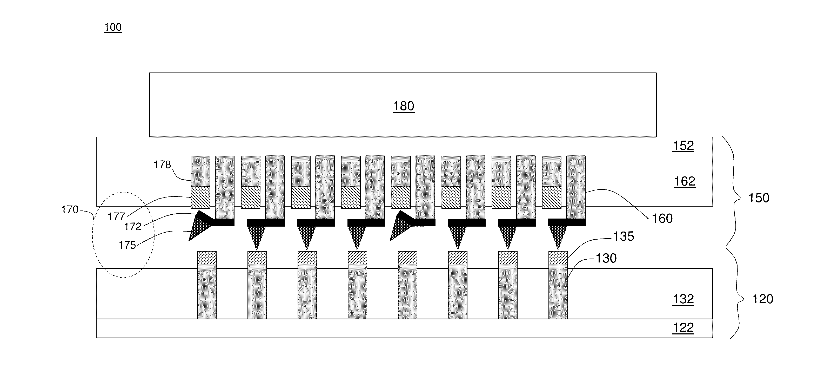
[0018]As stated above, there remains a need to functionally test portions of a 3-dimensional integrated circuit (IC) that are disposed within a single layer, before the single layer is permanently joined to a second layer of the 3-dimensional IC.

[0019]Exemplary embodiments may use a test probe chip, including a second IC layer, to test the functi...


PUM


Abstract

A test system for testing a multilayer 3-dimensional integrated circuit (IC), where two separate layers of IC circuits are temporarily connected in order to achieve functionality, includes a chip under test with a first portion of the 3-dimensional IC, and a test probe chip with a second portion of the 3-dimensional IC and micro-electrical-mechanical system (MEMS) switches that selectively complete functional circuits between the first portion of the 3-dimensional IC in a first IC layer to circuits within the second portion of the 3-dimensional IC in a second IC layer. The MEMS switches include tungsten (W) cone contacts, which make the selective electrical contacts between circuits of the chip under test and the test probe chip and which are formed using a template of graded borophosphosilicate glass (BPSG).

Description

BACKGROUND[0001]1. Field of the Invention[0002]The embodiments generally relate to functional testing of a multilayer 3-dimensional integrated circuit (IC), where two separate layers of IC circuits are temporarily connected in order to achieve functionality. More specifically, the embodiments relate to testing a portion of a 3-dimensional IC that is disposed within a chip under test, which includes a first IC layer, by employing a test probe chip including another portion of the 3-dimensional IC in a second IC layer and micro-electrical-mechanical system (MEMS) switches that selectively complete functional circuits, which span the first and second IC layers. Yet more specifically, the MEMS switches include tungsten (W) cone contacts that are formed using a template of graded borophosphosilicate glass (BPSG).[0003]2. Description of Related Art[0004]Three dimensional integrated circuits (ICs) include a number of advantages: shorter interconnects, which provide less delay and require l...

Claims


Application Information

Patent Timeline
IPC IPC(8): G01R1/067H01L21/768
CPCH01L22/14H01L21/76885H01L23/481H01L21/76804G01R1/06727G01R1/06738G01R1/06744H01L2924/0002G01R1/07342G01R3/00B81C1/00111B81B2203/0118H01L2924/00
Inventor ELLIS-MONAGHAN, JOHN J.GAMBINO, JEFFREY P.PETERSON, KIRK D.RANKIN, JED H.
Owner IBM CORP
Why Eureka
Try Eureka