Semiconductor substrate and semiconductor device and manufacturing method of the same

a semiconductor device and semiconductor technology, applied in the direction of semiconductor devices, basic electric elements, electrical equipment, etc., can solve the problems of unstable operation of a semiconductor device formed over the glass substrate, inability to provide a semiconductor layer, and low allowable temperature limit of such a glass substrate, etc., to achieve stable operation, reduce yield, and increase the effect of area

Inactive Publication Date: 2011-08-09
SEMICON ENERGY LAB CO LTD
View PDF13 Cites 3 Cited by
  • Summary
  • Abstract
  • Description
  • Claims
  • Application Information

AI Technical Summary

Benefits of technology

By provision of the film formed of PSG, BSG, or BPSG by the thermal CVD method using organosilane as one material source at a temperature equal to or higher than 500° C. and equal to or lower than 800° C., the semiconductor layer can be attached to the base substrate such as a glass substrate (bonding can be formed between the base substrate and such a film). Further, the film formed of one or a plurality of PSG, BSG, and BPSG by the thermal CVD method using organosilane as one material source at a temperature equal to or higher than 500° C. and equal to or lower than 800° C. is a film having a very smooth surface, and therefore, strong bonding can be formed by thermal treatment at a temperature equal to or lower than 700° C. According to this structure, an SOI layer having a bonding portion with high bonding strength can be obtained even over a base substrate the allowable temperature limit of which is 700° C. or less. Further, since the layer containing one or a plurality of PSG, BSG, and BPSG exists between the base substrate and the SOI layer, the SOI layer can be prevented from being adversely affected by highly mobile impurity ions which might be contained in the base substrate, and the operation of a semiconductor device manufactured using the SOI layer can be stably maintained. Further, the bonding layer also functions as a blocking layer for preventing impurity diffusion, so that increase of the number of manufacturing steps or a drop in yield can be reduced.
By using the semiconductor layer provided for such a substrate, high-performance semiconductor devices including various semiconductor elements, memory elements, integrated circuits, and the like can be manufactured with high yield.

Problems solved by technology

However, the allowable temperature limit of such a glass substrate is generally low and thermal treatment at a high temperature equal to or higher than 1000° C. is needed to strengthen bonding between a separated semiconductor layer and a silicon substrate in the method for manufacturing a semiconductor substrate by a conventional hydrogen-ion-implantation separation method.
Therefore, the glass substrate has not been able to be provided with a semiconductor layer having a bonding strength high enough for practical use by the conventional hydrogen-ion-implantation separation method.
Furthermore, in the case of the above-described glass substrate, there is also a problem in that highly mobile impurity ions of sodium or the like exist in the glass substrate and the operation of a semiconductor device formed over the glass substrate is made to be unstable by the impurity ions.

Method used


Image

  • Semiconductor substrate and semiconductor device and manufacturing method of the same
  • Semiconductor substrate and semiconductor device and manufacturing method of the same
  • Semiconductor substrate and semiconductor device and manufacturing method of the same

Examples


embodiment mode 1

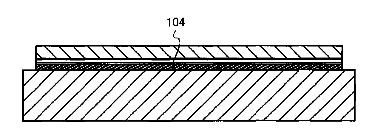
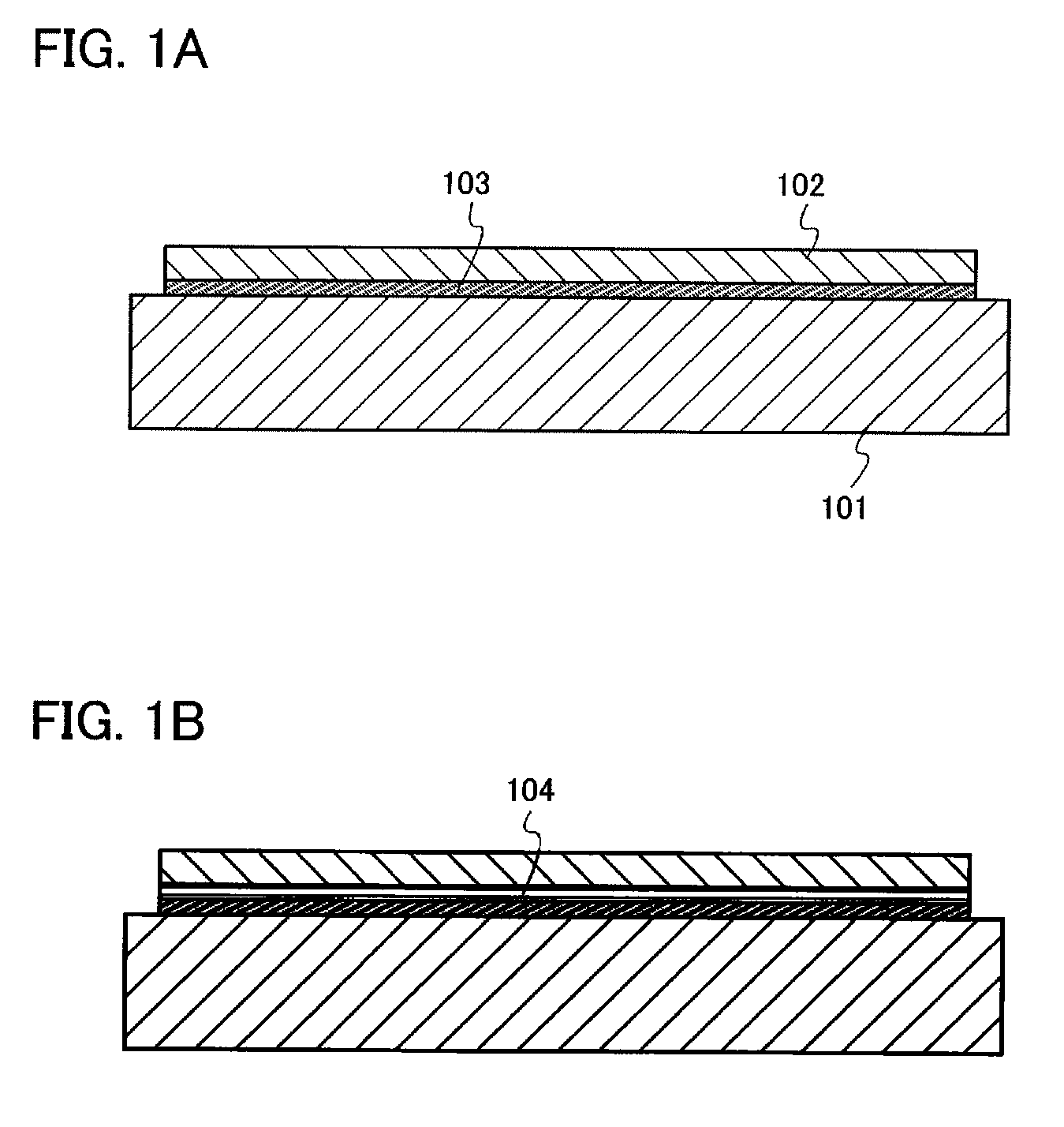
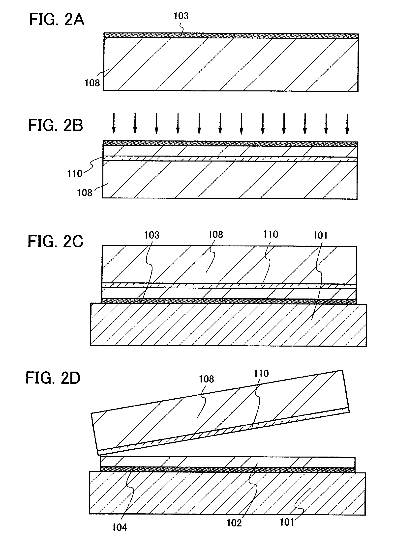
FIGS. 1A and 1B each show a semiconductor substrate according to the present invention. Note that, in this specification, a semiconductor substrate refers to a substrate in which a semiconductor layer is provided over a substrate having an insulating surface or an insulating substrate. Although the semiconductor layer is a single crystal semiconductor layer in many cases, a layer made of a polycrystal or a compound semiconductor may be used as well.

In FIG. 1A, a base substrate 101 is a substrate having an insulating surface or an insulating substrate, and any of a variety of glass substrates that are used in the electronics industry, such as an aluminosilicate glass substrate, an aluminoborosilicate glass substrate, and a barium borosilicate glass substrate, can be used. As the glass substrate, it is preferable to use a glass substrate having a coefficient of thermal expansion which is equal to or higher than 25×10−7 / ° C. and equal to or lower than 50×10−7 / ° C. (more preferably, equ...

embodiment mode 2

In this embodiment mode, a CMOS (complementary metal oxide semiconductor) will be described as an example of the semiconductor device of the present invention, using FIGS. 4A to 4E and FIGS. 5A to 5D. A method for manufacturing the semiconductor device will be described at the same time. According to this embodiment mode, a CMOS is manufactured using the semiconductor substrate described in Embodiment Mode 1 so that a CMOS with high performance and stable operation can be provided. Note that repetitive description for the same components as or components having similar functions to the components in Embodiment Mode 1 is omitted.

In FIG. 4A, the bonding layer 103, the barrier layer 104, and the semiconductor layer 130 are formed over the base substrate 101. Although the semiconductor substrate in which the barrier layer 104 for preventing one or both of phosphorus and boron contained in the bonding layer 103 from diffusing into the semiconductor layer is provided in this embodiment mo...

embodiment mode 3

In this embodiment mode, a liquid crystal display device will be described as an example of the semiconductor device of the present invention, using FIGS. 6A and 6B. According to this embodiment mode, a liquid crystal display device is manufactured using the semiconductor substrate described in Embodiment Mode 1 so that a liquid crystal display device with high performance and stable operation can be provided.

FIG. 6A is a top view of the liquid crystal display device, and FIG. 6B is a cross-sectional view of FIG. 6A taken along line C-D.

As shown in FIG. 6A, a pixel region 306 and driver circuit regions 304a and 304b which are scanning line driver circuits are sealed between a base substrate 310 and a counter substrate 395 with a sealant 392. A driver circuit region 307 which is a signal line driver circuit including a driver IC is provided over the base substrate 310. A transistor 375 and a capacitor 376 are provided in the pixel region 306. A driver circuit including transistors 37...


PUM

PropertyMeasurementUnit
temperatureaaaaaaaaaa

Abstract

A semiconductor substrate having an SOI layer is provided. Between an SOI layer and a glass substrate, a bonding layer is provided which is formed of one layer or a plurality of layers of phosphosilicate glass, borosilicate glass, and / or borophosphosilicate glass, using organosilane as one material by a thermal CVD method at a temperature of 500° C. to 800° C.

Description

BACKGROUND OF THE INVENTION1. Field of the InventionThe present invention relates to a method for manufacturing semiconductor substrates each having an SOI (silicon on insulator) structure in which a semiconductor layer is provided on an insulating surface and a method for manufacturing semiconductor devices each having an SOI structure.2. Description of the Related ArtIn recent years, development of electric appliances and electronic devices has not been stopped and higher-speed semiconductor devices have been demanded. Further, with development of portable devices and increasing of energy demand, decreasing of power consumption is also one big development theme. Due to such a background, as compared to a semiconductor device manufactured using a bulk silicon substrate, an SOI technology capable of providing a high-speed, low-power-consumption semiconductor device has attracted attention. The SOI technology is a technology in which a substrate having a structure in which a thin sem...

Claims


Application Information

Patent Timeline
Patent Type & Authority Patents(United States)
IPC IPC(8): H01L21/30
CPCH01L21/2007H01L21/321H01L21/76254H01L27/1214H01L27/1266H01L29/66772
Inventor KAKEHATA, TETSUYA
Owner SEMICON ENERGY LAB CO LTD
Why Eureka
Try Eureka