Method for manufacturing double-sided PERC high-efficiency crystalline silicon solar cell

A solar cell and manufacturing method technology, which is applied to circuits, photovoltaic power generation, electrical components, etc., can solve the problems of increased production cost, low battery utilization rate, inability to achieve work efficiency, etc., and achieves reduced manufacturing cost, convenient operation, and improved open circuit. The effect of voltage Uoc

Inactive Publication Date: 2019-04-05
RENESOLA JIANGSU LTD
View PDF1 Cites 3 Cited by
  • Summary
  • Abstract
  • Description
  • Claims
  • Application Information

AI Technical Summary

Problems solved by technology

In the existing single-sided PERC cells, the aluminum paste is printed on the entire back of the silicon wafer by printing, and the aluminum layer is completely covered on the laser etching line, and a local aluminum-silicon alloy layer is formed in the area of ​​the laser etching line. The place where the etched line is simply covered on the passivation film layer, because the all-aluminum back field is opaque, so the entire back cannot receive light to achieve back power generation, and only the front can absorb light energy to achieve single-side power generation, increasing the The production cost is low and the utilization rate of the produced battery is low, and the expected work efficiency cannot be achieved. In order to improve work efficiency, reduce production cost, save time and effort, and save energy, the present invention proposes a double-sided PERC high-efficiency crystalline silicon solar cell. method

Method used


Image

  • Method for manufacturing double-sided PERC high-efficiency crystalline silicon solar cell
  • Method for manufacturing double-sided PERC high-efficiency crystalline silicon solar cell

Examples


Embodiment 1

[0048] This embodiment provides a method for manufacturing a double-sided PERC high-efficiency crystalline silicon solar cell. The method is suitable for the manufacture of all P-type double-sided PERC high-efficiency crystalline silicon solar cells and includes the following steps:

[0049] (1) The crystalline silicon is textured in advance, and the surface reflectivity of the silicon wafer is controlled at 11% after texturing;

[0050] (2) Diffusion: crystalline silicon diffuses, and the diffusion resistance is 90Ω / □;

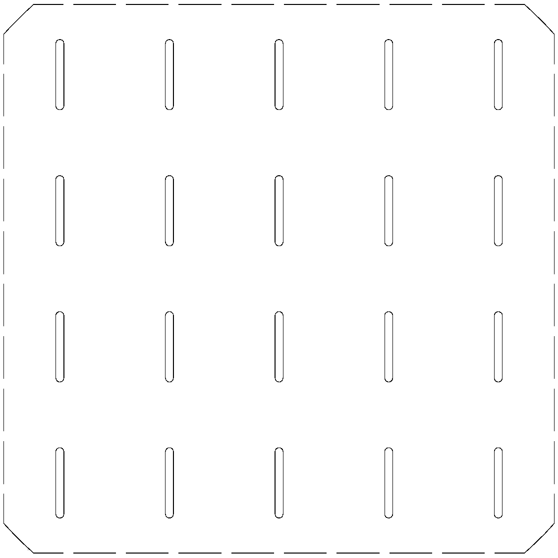
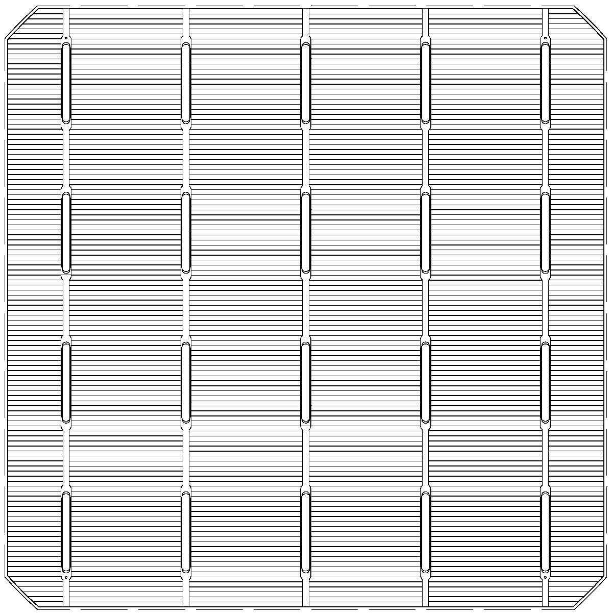
[0051] (3) Laser doping: Laser doping the diffused crystalline silicon to form the corresponding N++ layer. The line width of the secondary gate line in the laser doped area is 70μm, and the number is 108; the main gate line is perpendicular to the secondary gate Line, the width of a single main grid line is 0.7mm;

[0052] (4) Etching: After removing the diffused borophosphosilicate glass, the back reflectivity is controlled at 25%;

[0053] (5) Back passivation: pro...

Embodiment 2

[0058] This embodiment provides a method for manufacturing a double-sided PERC high-efficiency crystalline silicon solar cell. The method is suitable for the manufacture of all P-type double-sided PERC high-efficiency crystalline silicon solar cells and includes the following steps:

[0059] (1) The crystalline silicon is textured in advance, and the surface reflectance of the silicon wafer is controlled at 15% after texturing;

[0060] (2) Diffusion: crystalline silicon diffuses, and the diffusion resistance is 100Ω / □;

[0061] (3) Laser doping: laser doping the diffused crystalline silicon to form the corresponding N++ layer. The line width of the secondary gate line in the laser doped area is 90μm, and the number of lines is 108; the main gate line is perpendicular to the secondary gate Line, the width of a single main grid line is 0.7mm;

[0062] (4) Etching: After removing the diffused borophosphosilicate glass, the back reflectivity is controlled at 28%;

[0063] (5) Back passiva...

Embodiment 3

[0068] This embodiment provides a method for manufacturing a double-sided PERC high-efficiency crystalline silicon solar cell. The method is suitable for the manufacture of all P-type double-sided PERC high-efficiency crystalline silicon solar cells and includes the following steps:

[0069] (1) The crystalline silicon is textured in advance, and the surface reflectance of the silicon wafer is controlled at 13% after texturing;

[0070] (2) Diffusion: crystalline silicon diffuses, and the diffusion resistance is 95Ω / □;

[0071] (3) Laser doping: Laser doping the diffused crystalline silicon to form the corresponding N++ layer. The line width of the secondary gate line in the laser doped area is 80μm, and the number of lines is 108; the main gate line is perpendicular to the secondary gate Line, the width of a single main grid line is 0.7mm;

[0072] (4) Etching: After removing the diffused borophosphosilicate glass, the back reflectivity is controlled at 26%;

[0073] (5) Back passivat...


PUM


Abstract

The invention discloses a method for manufacturing a double-sided PERC high-efficiency crystalline silicon solar cell. The method comprises the following steps of (1) texturing, (2) diffusion including crystalline silicon diffusion, (3) laser doping including the laser doping of a diffused crystalline silicon, (4) etching including the removal of diffused borophosphosilicate glass, (5) back passivation including the production of a SiO2-Al2O3-SiNx:H laminated passivation film with a thickness of 80-100 nm, (6) front side film coating including the generation of a SiO2-SiNx anti-reflection filmwith thickness of 80-90 nm by using the PECVD technology, (7) Backside laser doping and trenching including the formation of a corresponding P++ layer, wherein the line width of each of 120 laser doped region sub-gate lines is 40-45 micrometers, and composite 1.6 mm main grids are set, and (8) backside printing including the formation of a back aluminum grid pattern, the collection of current andsintering to form the double-sided PERC high-efficiency crystalline silicon solar energy battery.

Description

Technical field [0001] The invention relates to the technical field of solar cell production and manufacturing, in particular to a method for manufacturing a double-sided PERC high-efficiency crystalline silicon solar cell. Background technique [0002] Conventional fossil fuels are increasingly depleted, and people's attention has been focused on solar energy. Solar energy, as an inexhaustible form of energy, is gradually entering our daily lives. At present, silicon-based solar cells are the most used cells on the market, and their high-efficiency power generation efficiency and mature production technology make photovoltaic parity grid a reality. However, with the development of technology, PERC cells, that is, passive emitter back-contact solar cells, have received extensive attention. In the existing single-sided PERC cell, the aluminum paste is printed on the entire backside of the silicon wafer by printing, and the aluminum layer is entirely covered on the laser etching ...

Claims


Application Information

Patent Timeline
Patent Type & Authority Applications(China)
IPC IPC(8): H01L31/18H01L31/0224
CPCH01L31/022441H01L31/1804Y02E10/547Y02P70/50
Inventor 赫汉马建峰葛祖荣
Owner RENESOLA JIANGSU LTD
Why Eureka
Try Eureka