Switching regulator

a switching regulator and regulator technology, applied in the direction of electric variable regulation, process and machine control, instruments, etc., can solve the problems of insufficient improvement of efficiency in the conventional switching regulator, loss of inductor hysteresis, loss of inductor current,

Inactive Publication Date: 2013-08-15
FUJITSU SEMICON LTD
View PDF11 Cites 52 Cited by
  • Summary
  • Abstract
  • Description
  • Claims
  • Application Information

AI Technical Summary

Problems solved by technology

A variety of losses are included in the power loss of the switching regulator.
For example, the losses include an inductor current loss and an inductor hysteresis loss, as well as switching loss, conduction loss and gate charge loss in an output drive transistor.
Therefore, improvement in efficiency may be insufficient in the conventional switching regulator.

Method used


Image

  • Switching regulator
  • Switching regulator
  • Switching regulator

Examples


first embodiment

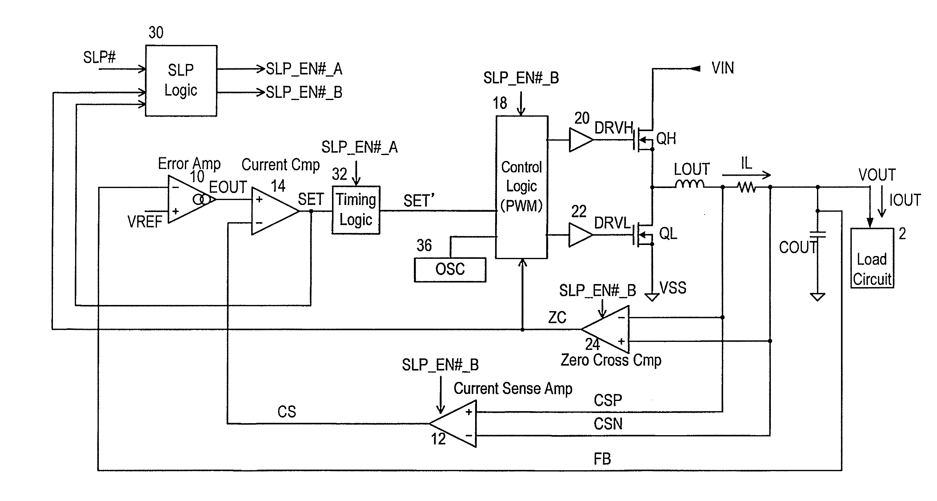
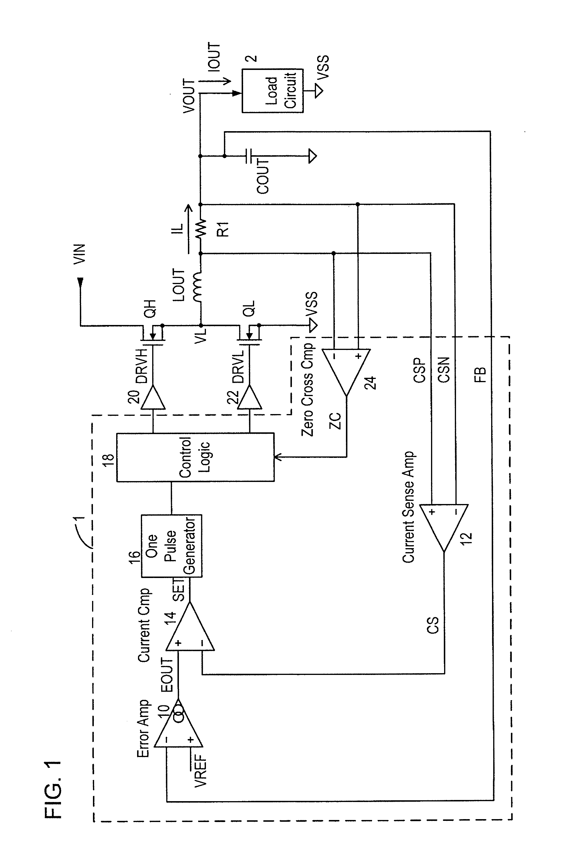
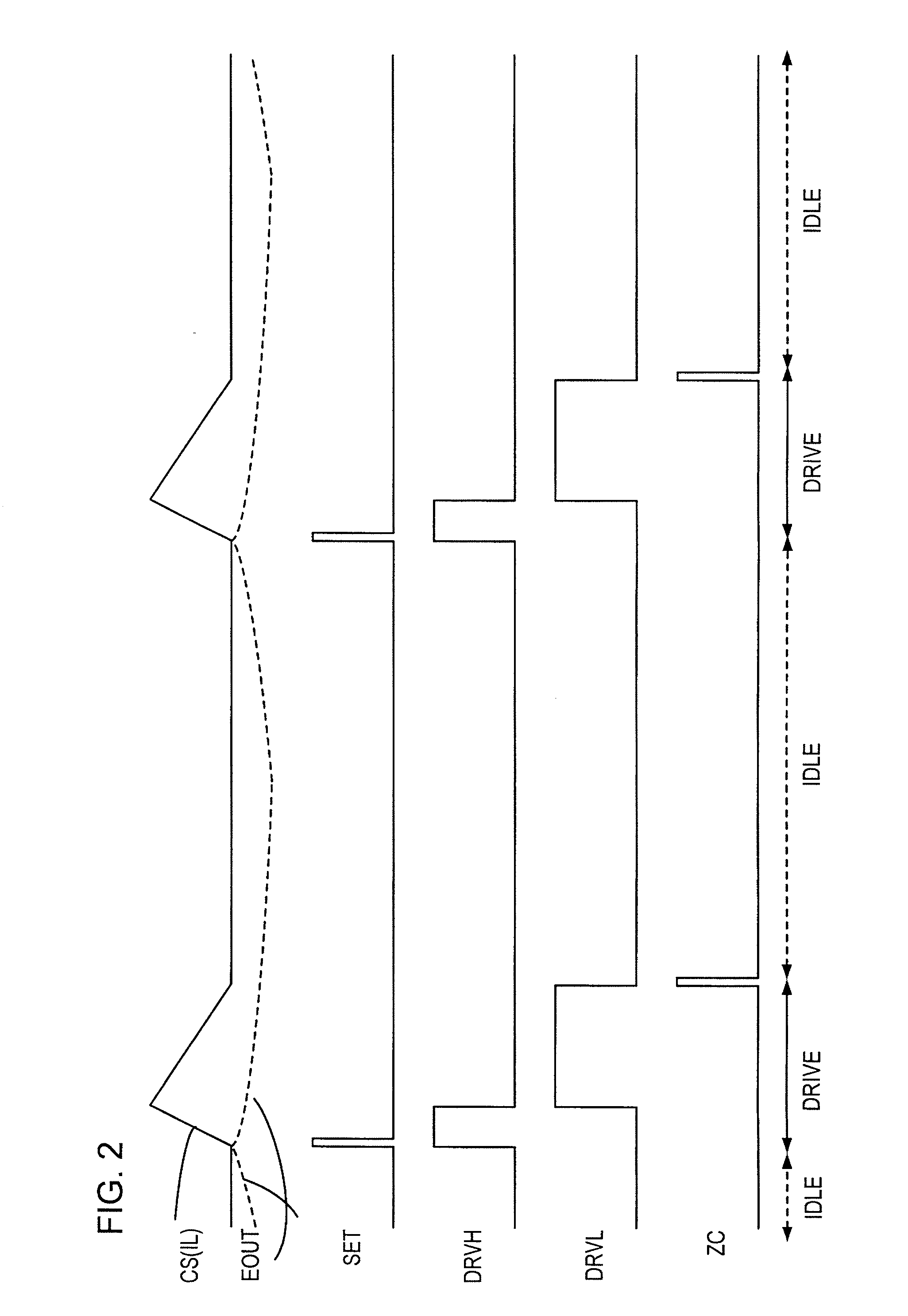
[0042]FIG. 4 is the configuration diagram of a switching regulator according to a first embodiment. The switching regulator stop or suspends the operation of a current sense amplifier 12 and a one pulse generation circuit 16 which generates a pulse CP is suspended (or minimizes the bias currents), when a sleep signal SLP# (where # signifies that an active state is produced when the signal of concern is in the L level), which guarantees a small load current and no occurrence of a sudden change in the load current, is received from either a load circuit 2 to which a second supply voltage VOUT is supplied or a control unit which controls the load circuit 2 (both together are designated as a load system). Here, an error amplifier 10 and a current comparator 14 are maintained to be in operational states, and further, when detecting a decrease of the second supply voltage VOUT supplied to the load circuit 2, the current sense amplifier 12 and the one pulse generation circuit 16 whose oper...

second embodiment

[0061]FIG. 8 is the configuration diagram of a switching regulator according to a second embodiment. FIG. 9 is a timing chart illustrating the operation of the switching regulator depicted in FIG. 8. In FIG. 8, a point of difference in configuration from the first embodiment depicted in FIG. 4 is that there are provided an ON-time timer circuit having a flip-flop 161 and a timer circuit 162 as the one pulse generation circuit 16, and further, an overcurrent protection circuit 26 and an overvoltage & undervoltage protection circuit 28. Other configuration is identical to the configuration depicted in FIG. 4. Here, the LSI chip 1 in the switching regulator is omitted in FIG. 8.

[0062]In the one pulse generation circuit 16, the flip-flop 161 is set in response to the trigger signal SET or SET′, so as to set the output Q to the H level. After a constant time W from the rise edge of the output Q, the timer circuit 162 sets an output to the H level, and in response thereto, the flip-flop 1...

third embodiment

[0070]FIG. 10 is the configuration diagram of a switching regulator according to a third embodiment. In FIG. 10, the LSI chip 1 of the switching regulator is omitted. In FIG. 10, a point of difference in configuration from FIG. 4 is that the current comparator includes two current comparators 14-1, 14-2. A first current comparator 14-1 is a circuit capable of fast responding to an input variation, while a second current comparator 14-2 is a circuit with a slower response speed than the first current comparator 14-1.

[0071]FIG. 11 illustrates circuit diagrams of the current comparators 14-1, 14-2, respectively. The two circuits are of equivalent configuration, each including: PMOS transistors P1, P2 which compare the output voltage EOUT with CS; PMOS transistors P3, P4 connected as the loads of the PMOS transistors P1, P2; and an output PMOS transistor P5 whose gate is connected to the drain terminal of the PMOS transistor P2. Further, each current comparator includes: a bias current ...


PUM


Abstract

A switching regulator controls an output transistor supplying current to an inductor and generates a second supply voltage from a first supply voltage. The switching regulator has: an error amplifier amplifying a difference between the second supply voltage and a reference voltage; a current sense amplifier converting an inductor current into voltage; a current comparator comparing an output voltages of the error amplifier and the current sense amplifier, so as to output a trigger signal when the second supply voltage decreases; a pulse generation circuit generating a control pulse to drive the first output transistor in response to the trigger signal; and a sleep control circuit, during a sleep period by a sleep signal supplied from a load side, suspending operation of the current sense amplifier or the pulse generation circuit, and tentatively resuming the suspended operation in response to the trigger signal, and thereafter suspending the operation again.

Description

CROSS-REFERENCE TO RELATED APPLICATION[0001]This application is based upon and claims the benefit of priority of the prior Japanese Patent Application No. 2012-025669, filed on Feb. 9, 2012, the entire contents of which are incorporated herein by reference.FIELD[0002]The embodiment relates to a switching regulator.BACKGROUND[0003]A switching regulator generates from an input first supply voltage a second supply voltage to be supplied to a load circuit, and supplies the generated voltage thereto. The switching regulator is intended to maintain the second supply voltage to a specified voltage in both a heavy load condition in which a large current is consumed in the load circuit and a light load condition in which a small current is consumed.[0004]In another aspect, from a demand of low power consumption in the switching regulator mounted on, for example, mobile equipment or the like, it is preferable to suppress power consumption in the internal circuit of the switching regulator, so...

Claims


Application Information

Patent Timeline
Patent Type & Authority Applications(United States)
IPC IPC(8): G05F1/10
CPCG05F1/10H02M3/158H02M1/0009H02M1/0032Y02B70/10
Inventor FUTAMURA, KAZUYOSHI
Owner FUJITSU SEMICON LTD
Why Eureka
Try Eureka