
Efficient and directed nano-light emitting diode, and method for making same

a light-emitting diode and efficient technology, applied in the field of light-emitting devices, can solve the problems of reducing efficiency, affecting the efficiency of light-emitting diodes, and the loss of most of light emitted within semiconductor led materials, and achieve the effect of increasing light extraction efficiency and large light extraction efficiency

Active Publication Date: 2013-08-29
RENESSELAER POLYTECHNIC INST
View PDF2 Cites 4 Cited by
  • Summary
  • Abstract
  • Description
  • Claims
  • Application Information

AI Technical Summary

Benefits of technology

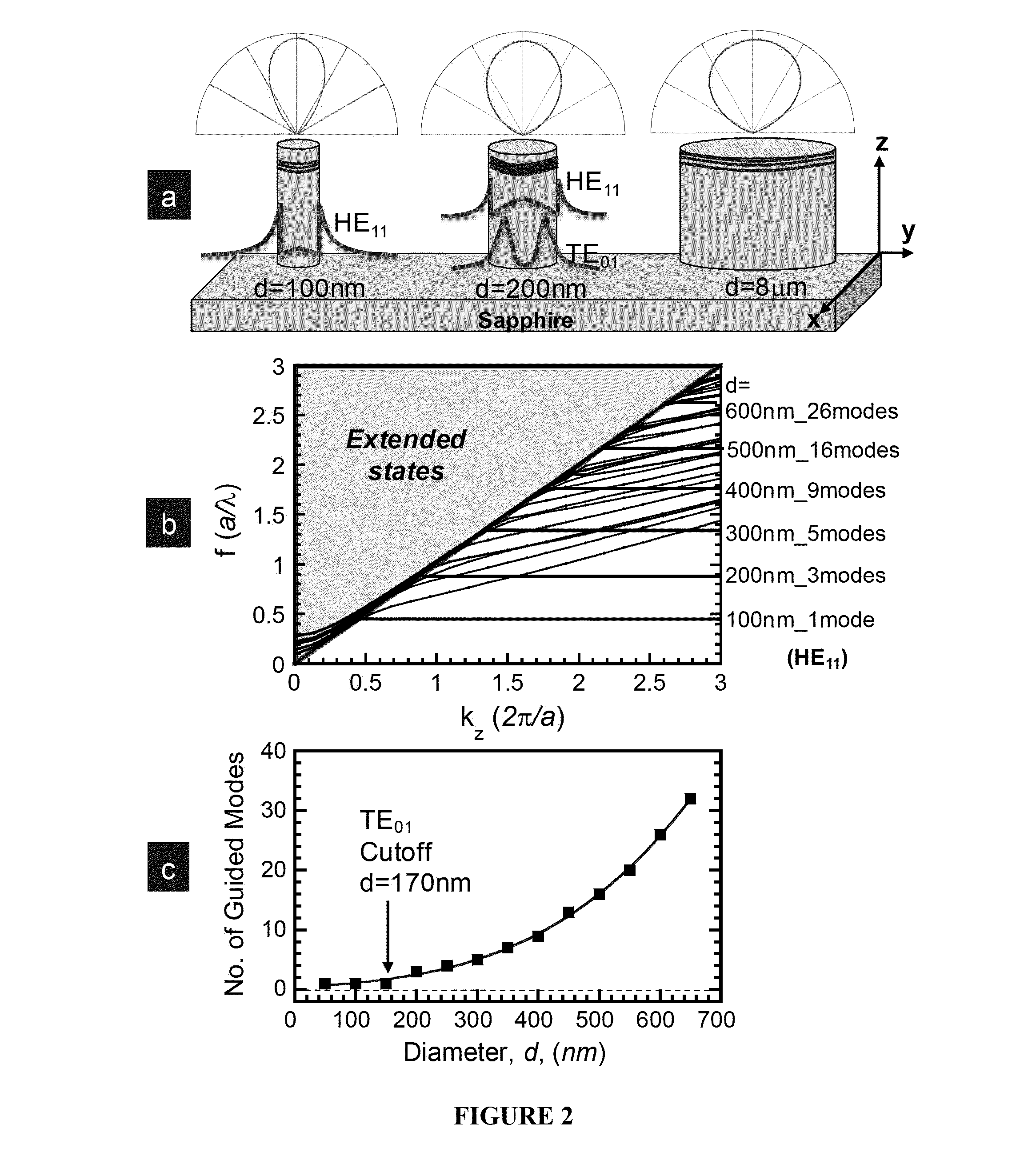
This patent describes a method for improving the efficiency of LEDs by using a special design that reduces the size of the LED and directs the light in a more directed way. This design uses a special type of light called a guided mode, which helps to increase the amount of light that comes out of the LED. This method doesn't require any additional tools or materials and can be used to make LEDs that are more efficient and directional.

Problems solved by technology

However, most of the light emitted within a semiconductor LED material is lost due to total internal reflection at the semiconductor-air interface.
Typical semiconductor materials have a high index of refraction, and thus, according to Snell's law, most of the light will remain trapped in the materials, thereby decreasing efficiency.
However, there have been few recent advances in the field of LED extraction.

Method used


Image

  • Efficient and directed nano-light emitting diode, and method for making same
  • Efficient and directed nano-light emitting diode, and method for making same
  • Efficient and directed nano-light emitting diode, and method for making same

Examples


examples

[0059]The invention, having been generally described, may be more readily understood by reference to the following examples, which are included merely for purposes of illustration of certain aspects and embodiments of the present invention, and are not intended to limit the invention in any way.

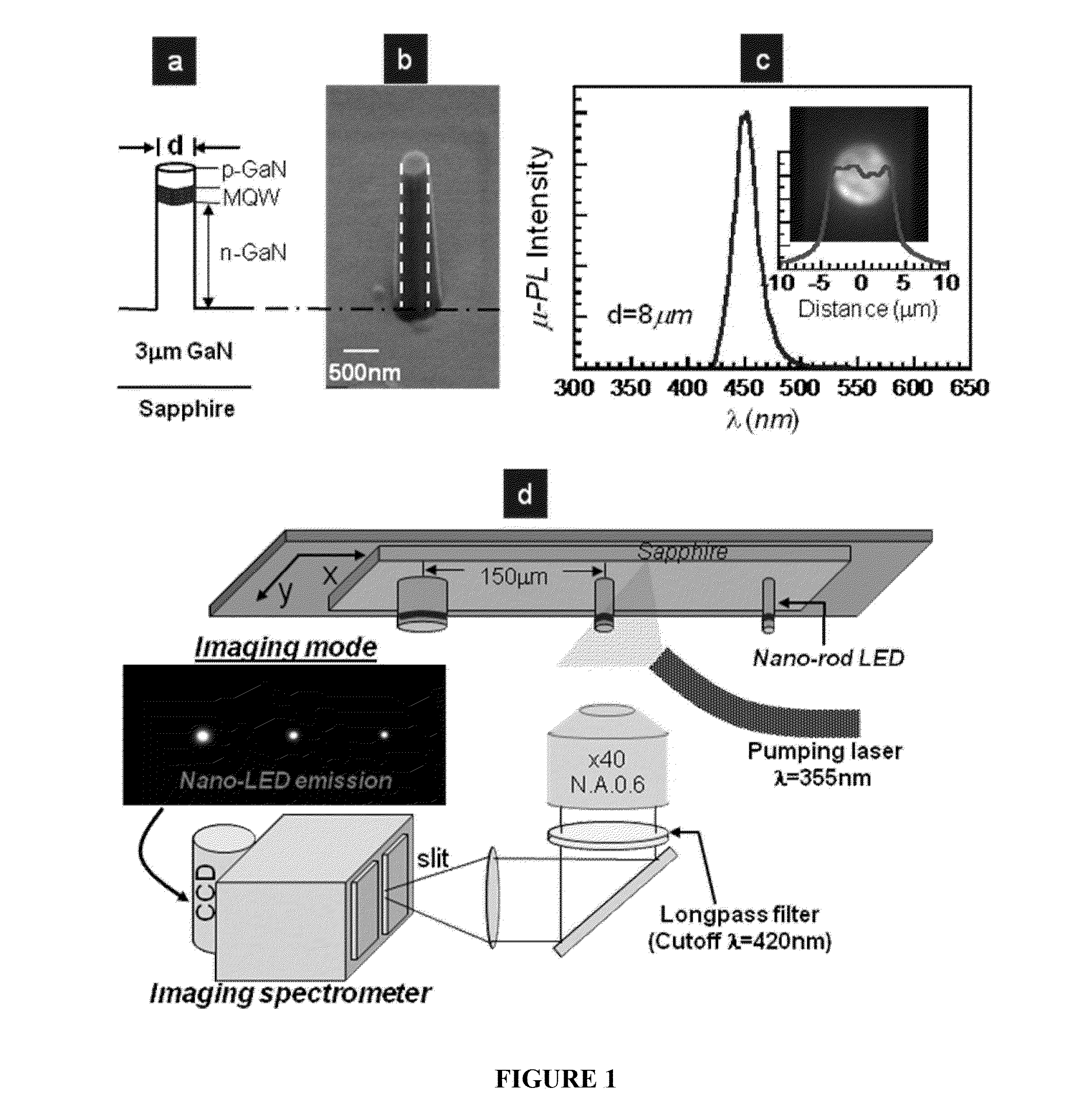
[0060]The LED sample was grown on a sapphire substrate. The multi-quantum-wells consist of six periods of In0.23Ga0.77N / GaN and are sandwiched between a 125 nm p-type GaN and 4 μm n-type and un-doped GaN layers. The nano-rod LED was produced using a direct electron-beam-write method followed by metal deposition (Nickel) and lift-off processes. The nano-rod had a diameter ranging from d=50 nm-8 μm and an etch depth of ˜1.4 μm. The detailed nanofabrication process is described in Huang, H. W., Kao, C. C., Hsueh, T. H., Yu, C.C., Lin, C. F., Chu, J. T., Kuo, H. C, Wang, S. C. “Fabrication of GaN-based nanorod light emitting diodes using self-assemble nickel nano-mask and inductively coupled plas...


PUM


Abstract

The invention relates to light-emitting devices, and related components, systems and methods. In one aspect, the present invention is related to light emitting diode (LED) light extraction efficiency. A non-limiting example, the application teaches a method for improving light emitting diode (LED) extraction efficiency, by providing a nano-rod light emitting diode; providing quantum wells; and reducing the size of said nano-rod LED laterally in the quantum-well plane (x and y), thereby improving LED extraction efficiency.

Description

CROSS-REFERENCE TO RELATED APPLICATIONS[0001]This application claims the benefit under 35 U.S.C. §119 of U.S. Provisional Patent Application No. 61 / 401,603, filed Aug. 16, 2010, the entire disclosure of which is incorporated herein by reference.STATE AND FEDERAL FUNDED RESEARCH[0002]The invention described herein was made with support of the National Service Foundation under Award Number EEC-0812056. The U.S. Government may have certain rights to this invention.TECHNICAL FIELD[0003]The invention relates to light-emitting devices, and related components, systems and methods. In one aspect, the present invention is related to light extraction efficiency of a light emitting diode (LED).BACKGROUND OF THE INVENTION[0004]A light emitting diode (LED) is a semiconductor device that emits light in a stimulated manner. This effect is a form of electroluminescence. LEDs can provide light in a more efficient manner than an incandescent and / or a fluorescent light source. The relatively high powe...

Claims


Application Information

Patent Timeline
Patent Type & Authority Applications(United States)
IPC IPC(8): H01L33/06H01L33/00
CPCH01L33/007H01L33/06H01L33/20Y10S977/95H01L33/005Y10S977/755Y10S977/89B82Y40/00H01L33/18
Inventor KUO, MEI-LINGLIN, SHAWN-YUKIM, YONG-SUNGHSIEH, MEI-LI
Owner RENESSELAER POLYTECHNIC INST
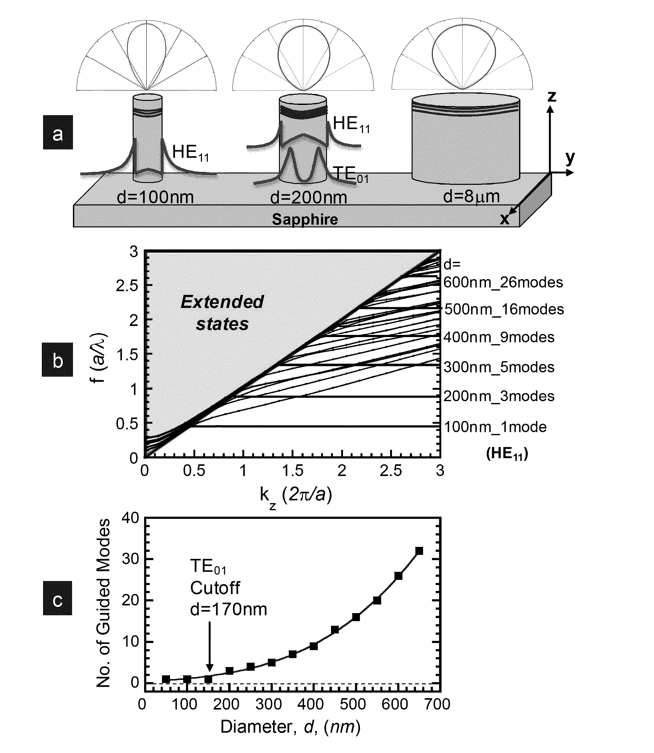
Learn More