Exposure apparatus and device manufacturing method using same
- Summary
- Abstract
- Description
- Claims
- Application Information
AI Technical Summary
Benefits of technology
Problems solved by technology
Method used
Image
Examples
Embodiment Construction
[0019]Hereinafter, preferred embodiments of the present invention will now be described in detail with reference to the accompanying drawings.
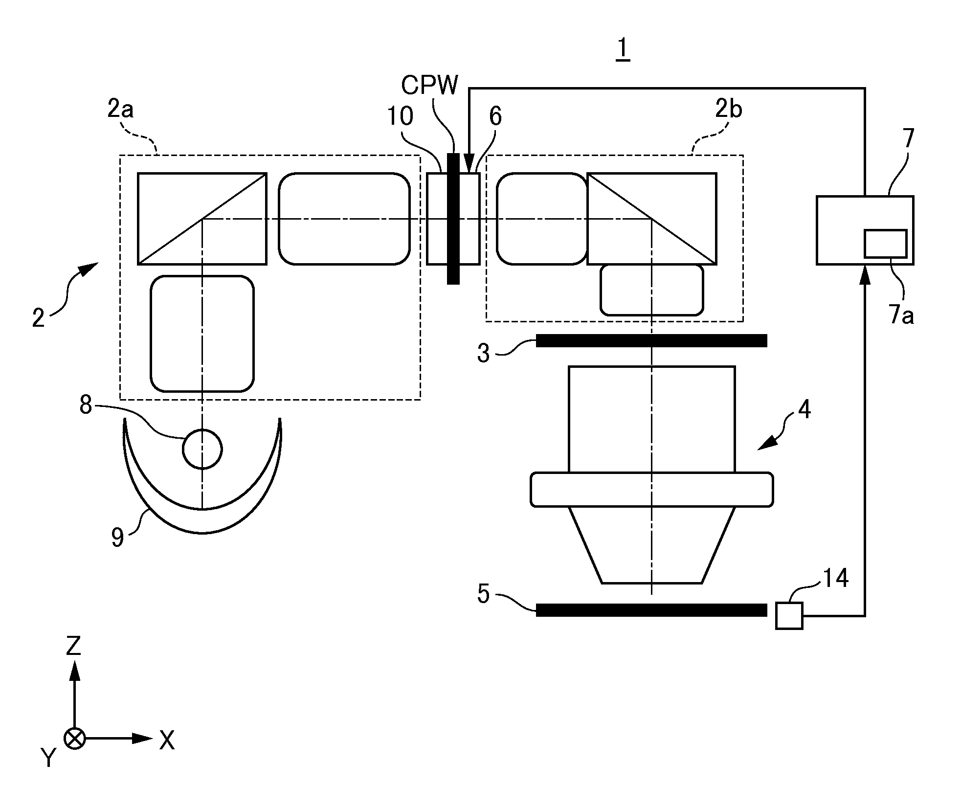
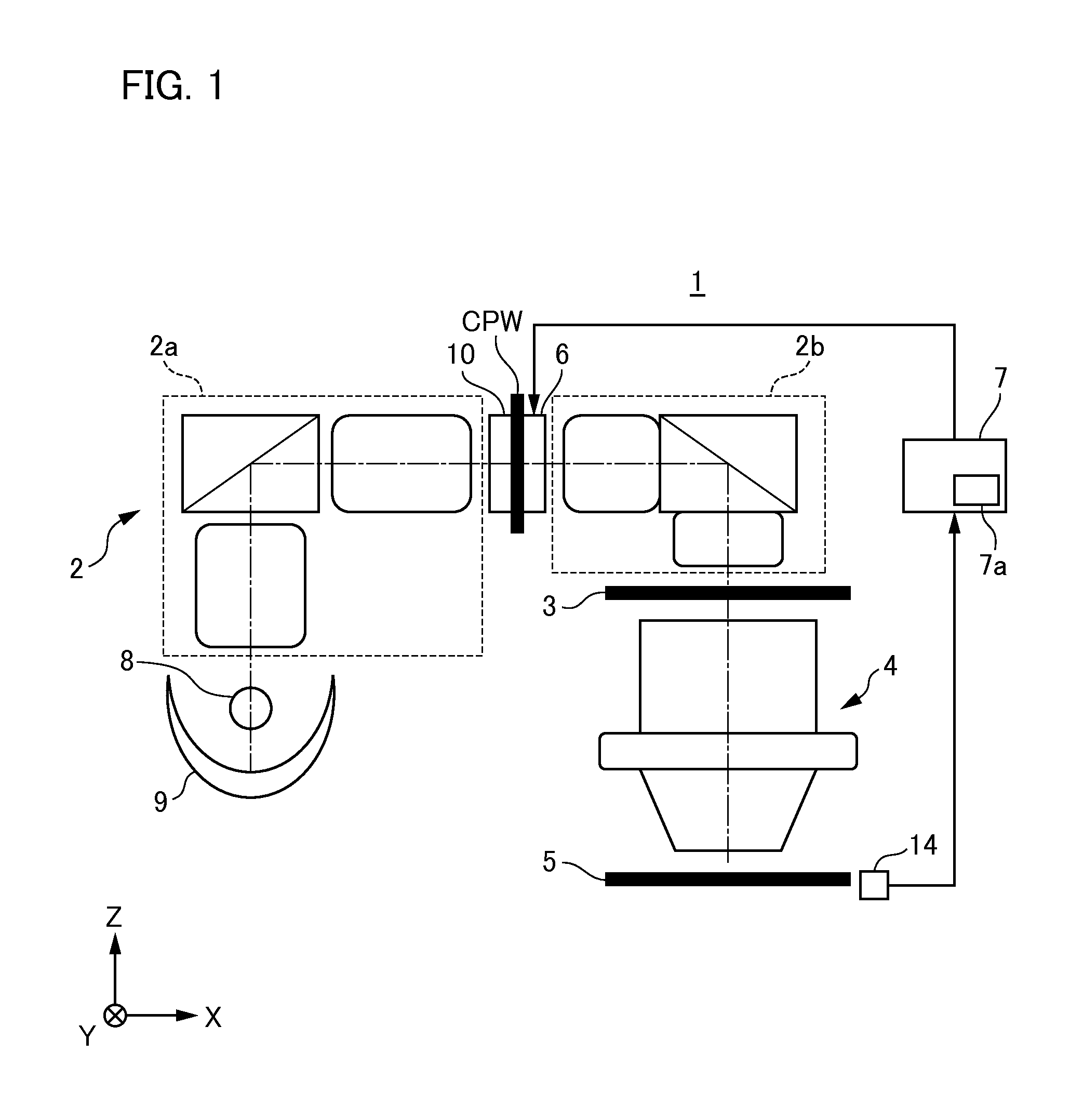
[0020]Firstly, a description will be given of the configuration of an exposure apparatus according to one embodiment of the present invention. The exposure apparatus of the present embodiment is used in a lithography step in the semiconductor device manufacturing steps and performs exposure processing on a wafer, i.e., a substrate. Hereinafter, the exposure apparatus is, for example, a projection exposure apparatus that employs a step-and-repeat system and projects and exposes a pattern formed on a reticle serving as an original plate on a wafer (substrate). FIG. 1 is a schematic diagram illustrating the configuration of an exposure apparatus 1 of the present embodiment. In FIG. 1, a description will be given where the Z axis is aligned parallel to the optical axis of a projection optical system, the Y axis is aligned in the scanning direction...
PUM
 Abstract
Description
Claims
Application Information


