Bond type flip-chip light-emitting structure and method of manufacturing the same

a technology of flip-chips and light-emitting structures, which is applied in the direction of semiconductor/solid-state device manufacturing, electrical equipment, semiconductor devices, etc., can solve the problems of large production costs, poor heat dissipation efficiency, and large negative electrode area, so as to reduce production costs, increase heat dissipation area, and increase light-emitting efficiency

Active Publication Date: 2013-09-12
PAITRIX
View PDF3 Cites 16 Cited by
  • Summary
  • Abstract
  • Description
  • Claims
  • Application Information

AI Technical Summary

Benefits of technology

[0011]A major objective of the present invention is to provide a bond type flip-chip light-emitting structure and method of manufacturing the same. Wherein, bonded metal layers replace the bonded tin balls, to reduce its production cost, while increasing its heat dissipation area, and raising its light emitting efficiency.
[0012]Another objective of the present invention is to provide a bond type flip-chip light-emitting structure and method of manufacturing the same, such that it can use an eutectic packaging process, to reduce the production cost effectively.

Problems solved by technology

In the flip-chip light-emitting structure of the prior art, a plurality of tin balls are used to connect LED to the substrate, that has the problem of poor heat dissipation and overly large negative electrode area.
Also, it has the shortcomings of complicated manufacturing process, requiring large machine to produce, and overly high packaging cost.

Method used


Image

  • Bond type flip-chip light-emitting structure and method of manufacturing the same
  • Bond type flip-chip light-emitting structure and method of manufacturing the same
  • Bond type flip-chip light-emitting structure and method of manufacturing the same

Examples


Embodiment Construction

[0021]The purpose, construction, features, functions and advantages of the present invention can be appreciated and understood more thoroughly through the following detailed description with reference to the attached drawings. And, in the following, various embodiments are described in explaining the technical characteristics of the present invention.

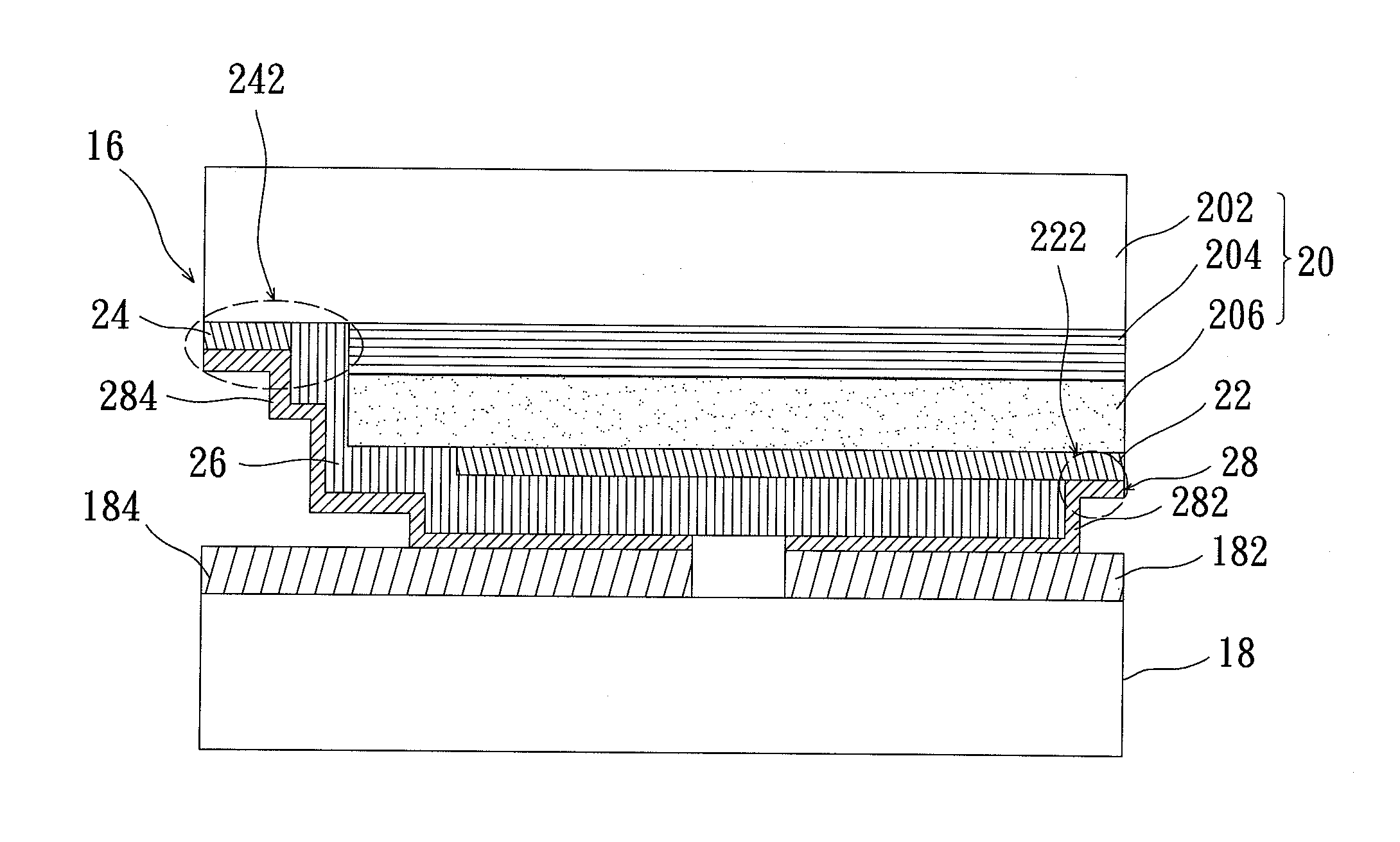
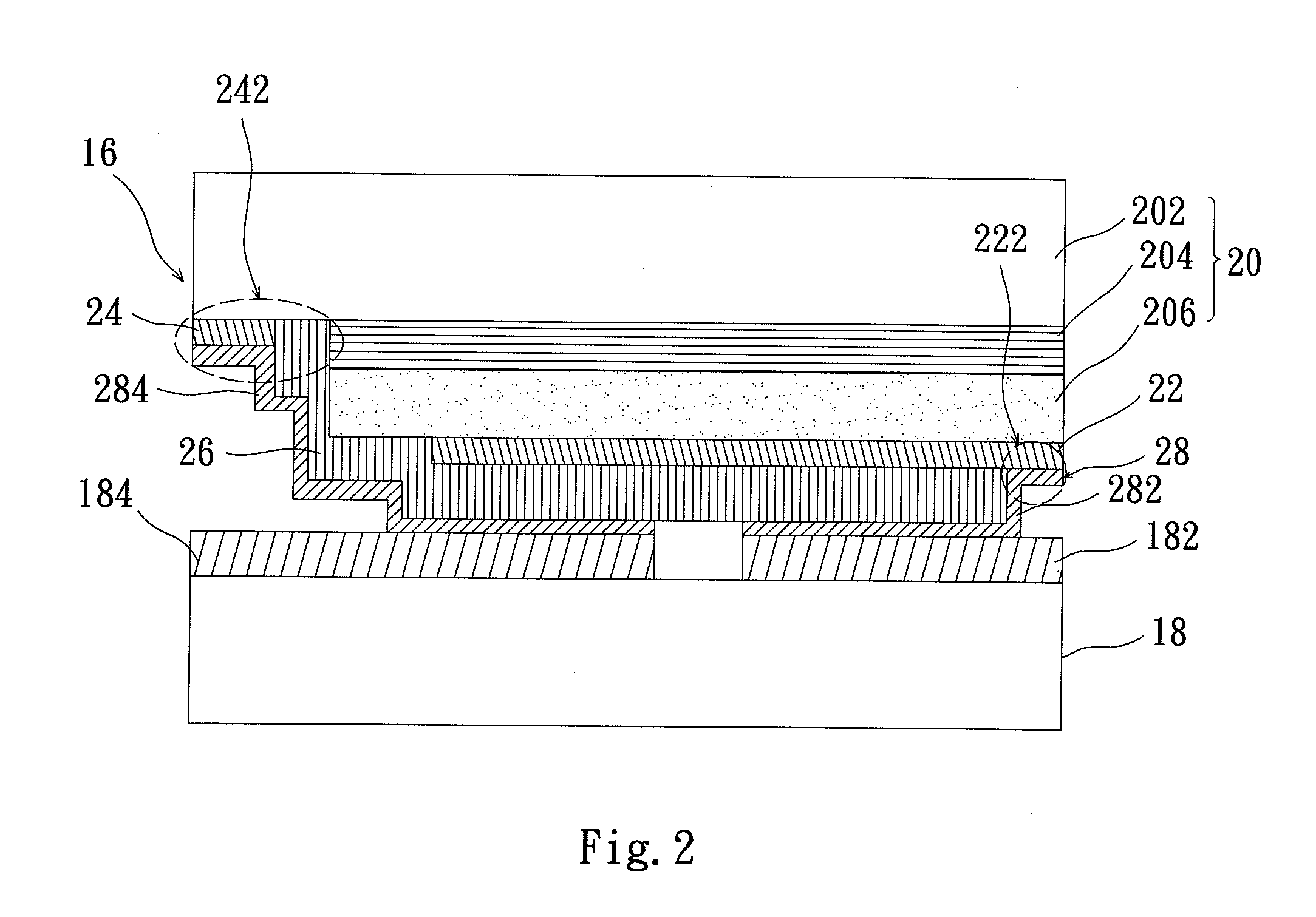
[0022]Firstly, refer to FIG. 2 for a schematic diagram of a bond type flip-chip light-emitting structure according to the present invention. As shown in FIG. 2, the bond type flip-chip light-emitting structure of the present invention includes, a light-emitting-diode (LED) 16 and a substrate 18. The LED 16 includes an epitaxy layer 20, a positive electrode 22, a negative electrode 24, an insulation layer 26, and a bonded metal layer 28. Wherein, the epitaxy layer 20 contains sequentially an n-type semiconductor layer 202, a multi-quantum-well light-emitting layer 204, and a p-type semiconductor layer 206. When driven by a voltage, the e...


PUM

PropertyMeasurementUnit
shapeaaaaaaaaaa
n-type semiconductoraaaaaaaaaa
heat dissipation capabilityaaaaaaaaaa

Abstract

A bond type flip-chip light-emitting structure and method of manufacturing the same. Firstly, form a positive electrode and a negative electrode on an epitaxy layer. Next, deposit an insulation layer on parts of the positive electrode and negative electrode, to expose respectively a positive electrode via hole and a negative electrode via hole. Then, form a bonded metal layer on the insulation layer, the positive electrode via hole, and the negative electrode via hole, so that the positive electrode and the negative electrode are on a same plane by means of the bonded metal layer. Finally, on a substrate, bond the first metal layer and the second metal layer onto the corresponding first bonded metal unit and the second bonded metal unit of the bonded metal layer, to form into shape, thus realizing a bond type flip-chip light-emitting structure.

Description

BACKGROUND OF THE INVENTION[0001]1. Field of the Invention[0002]The present invention relates to a bond type flip-chip light-emitting structure and method of manufacturing the same, and in particular to a bond type flip-chip light-emitting structure, that is realized through a light-emitting-diode (LED) made by bonding a metal layer and a substrate into shape, to increase its contact area effectively, hereby increasing its heat dissipation capability.[0003]2. The Prior Arts[0004]In recent years, the light-emitting-diode (LED) has been considered one of the most promising Industries, mainly for its advantages of compact size, high efficiency, fast response, long service life, and not containing mercury hazardous to the environment, thus it is suitable for high power illumination.[0005]However, the most important disadvantages of LED is its heat dissipation problem. To be more specific, when its light radiation efficiency is not good enough, such that the light that can not pass throu...

Claims


Application Information

Patent Timeline
Patent Type & Authority Applications(United States)
IPC IPC(8): H01L33/36H01L33/04
CPCH01L33/36H01L33/04H01L33/44H01L33/62H01L2924/0002H01L2924/00
Inventor CHANG, LIANN-BEXU, CHENXU, KUNZHANG, YUNYUNCHIEN, HOW-WEN
Owner PAITRIX
Why Eureka
Try Eureka