Semiconductor power device integrated with clamp diodes having dopant out-diffusion suppression layers

a technology of clamp diodes and power devices, applied in semiconductor devices, diodes, electrical apparatus, etc., can solve the problem of low esd capability, achieve the effect of enhancing esd capability, reducing power consumption, and degrading esd capability

Inactive Publication Date: 2013-09-12
FORCE MOS TECH CO LTD
View PDF2 Cites 7 Cited by
  • Summary
  • Abstract
  • Description
  • Claims
  • Application Information

AI Technical Summary

Benefits of technology

[0006]It is therefore an object of the present invention to provide a new an improved semiconductor power device configuration and manufacture method to solve the problems discussed above to benefit yield enhancement and achieve lower power consumption without degrading ESD capability or to enhance ESD capability without sacrificing yield by forming a dopant out-diffusion suppression layer containing Fluorine into upper portion of the Gate-Source clamp diode, wherein the dopant out-diffusion suppression layer comprises multiple alternating doped regions, for example, an array of n* / p* / n* / p* / n* regions formed into the upper portion of the Gate-Source clamp diode comprising an array of n+ / p / n+ / p / n+ regions in an N-channel trench MOSFET, wherein the n* region is n+ doped containing Fluorine and the p* region is p doped containing Fluorine. From Table 1 it can be seen that, by forming the inventive dopant out-diffusion suppression layer (ion implantation energy is 50 KeV and dose is 5.0E14cm2), the average Igss is reduced about 40% and the Igss standard deviation is reduced about 60% comparing with the prior arts while the average BVgss and the BVgss standard deviation is slightly reduced. The experiment results indicate that this invention benefits yield enhancement and low power consumption due to low Igss without degrading the ESD capability or enhances the ESD capability by increasing the Igss without sacrificing yield due to low Igss standard deviation.

Problems solved by technology

In the condition of prior arts, the yield becomes unstable as result of the Igss out of spec (e.g.>10 uA) when Vgs=20V, therefore in order to keep good yield, the average Igss is kept relatively low, however, the BVgss becomes higher, resulting in low ESD capability.
Therefore, the prior arts encounter a trade-off between the ESD capability and yield due to the limit of the Igss for less power consumption as mentioned above.

Method used


Image

  • Semiconductor power device integrated with clamp diodes having dopant out-diffusion suppression layers
  • Semiconductor power device integrated with clamp diodes having dopant out-diffusion suppression layers
  • Semiconductor power device integrated with clamp diodes having dopant out-diffusion suppression layers

Examples


Embodiment Construction

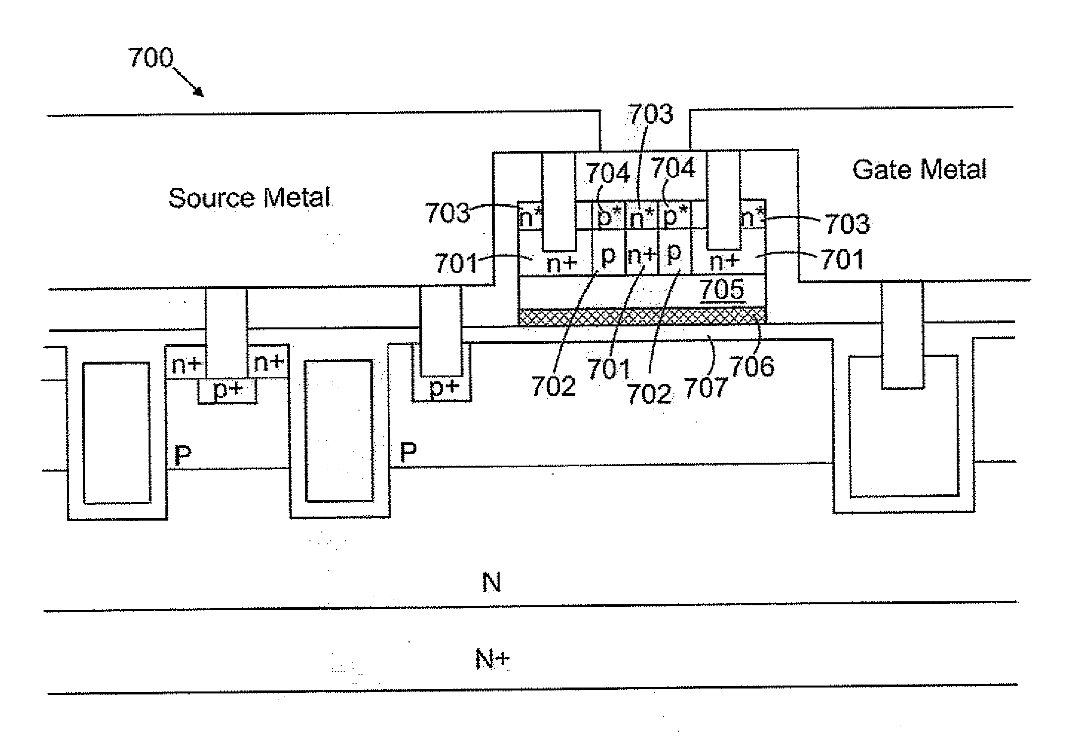
[0025]Please refer to FIG. 2 for a preferred embodiment in which an N-channel trench MOSFET 500 integrated with an Gate-Source clamp diode is disclosed, wherein the Gate-Source clamp diode comprises an array of alternating doped regions of n+ region 501 and p region 502. According to the present invention, an dopant out-diffusion suppression layer is formed into the upper portion of the Gate-Source clamp diode, composed of an array of alternating doped regions of n* region 503 and p* region 504, wherein the n* region 503 formed above the n+ region 501 is n+ doped containing Fluorine, and the p* region 504 formed above the p region 502 is p doped containing Fluorine. Furthermore, the Gate-Source clamp diode formed on a thin oxide layer 505 over an N epitaxial layer 506 is connected to a source metal 507 of the trench MOSFET 500 on one side and to a gate metal 508 of the trench MOSFET 500 on another side via planar diode contacts, wherein the source metal 507 is also contacting with n...


PUM


Abstract

A semiconductor power device integrated with clamp diodes is disclosed by offering dopant out-diffusion suppression layers to enhance the ESD protection between gate and source, and avalanche capability between drain and source.

Description

FIELD OF THE INVENTION[0001]This invention generally relates to improved MOSFET (Metal Oxide Semiconductor Field Effect Transistor) configuration or IGBT (Insulated Gate Bipolar Transistor) integrated with a Gate-Source clamp diode for ESD (Electrostatic Discharge) protection between gate and source, and a Gate-Drain clamp diode for avalanche protection between drain and source having dopant out-diffusion suppression layers to benefit the ESD and the avalanche protections.BACKGROUND OF THE INVENTION[0002]For a semiconductor power device, for example a trench MOSFET device integrated with a Gate-Source clamp diode, Igss and BVgss are key parameters to measure performance of the Gate-Source clamp diode, wherein the Igss defined by gate-source current at max.Vgs spec (maximum voltage spec between gate and source), e.g. 20V is usually kept below 10 uA and the BVgss is usually defined by the voltage drop between the gate and the source at Igss=300 uA. Besides, the ESD capability is highe...

Claims


Application Information

Patent Timeline
Patent Type & Authority Applications(United States)
IPC IPC(8): H01L27/06H01L21/20
CPCH01L27/0255H01L27/0629H01L29/417H01L29/41766H01L29/66106H01L29/167H01L29/66734H01L29/7808H01L29/7813H01L29/866H01L29/0653H01L29/66727
Inventor HSIEH, FU-YUAN
Owner FORCE MOS TECH CO LTD
Why Eureka
Try Eureka