Electronic component element housing package

Active Publication Date: 2013-09-19
SUMITOMO METAL SMI ELECTRONICS DEVICES
View PDF11 Cites 3 Cited by
  • Summary
  • Abstract
  • Description
  • Claims
  • Application Information

AI Technical Summary

Benefits of technology

[0012]One or more embodiments of the claimed invention provide an electronic component element housing package capable of increased bending strength of the ceramic substrate and capable of securing greater bond strength of the metalized layers formed by simultaneous firing wit

Problems solved by technology

Consequently, if the thickness of the ceramic substrate is reduced, the electronic component element housing package becomes unable to withstand thermal stress during metal cover bonding after electronic component mounting.
In addition, if the thickness is increased, after the electronic components are mounted this electronic component element housing package becomes unable to be used as a small, low-profile package capable of being mounted on module capable of supporting thinner and smaller sizes.
(1) The electronic component element housing package disclosed in Patent Document 1 is bonded with low-melting point glass as a seal with a lead terminal sandwiched between a ceramic substrate on which the electronic component elements are mounted and a cover, and differs completely from a package having a layered structure in which metal layers are formed in the ceramic substrate by simultaneous firing in a reducing atmosphere. For example, although it was possible to increase the bending strength by using a sintered body of alumina w

Method used


Image

  • Electronic component element housing package
  • Electronic component element housing package

Examples


Example

Working Example 1

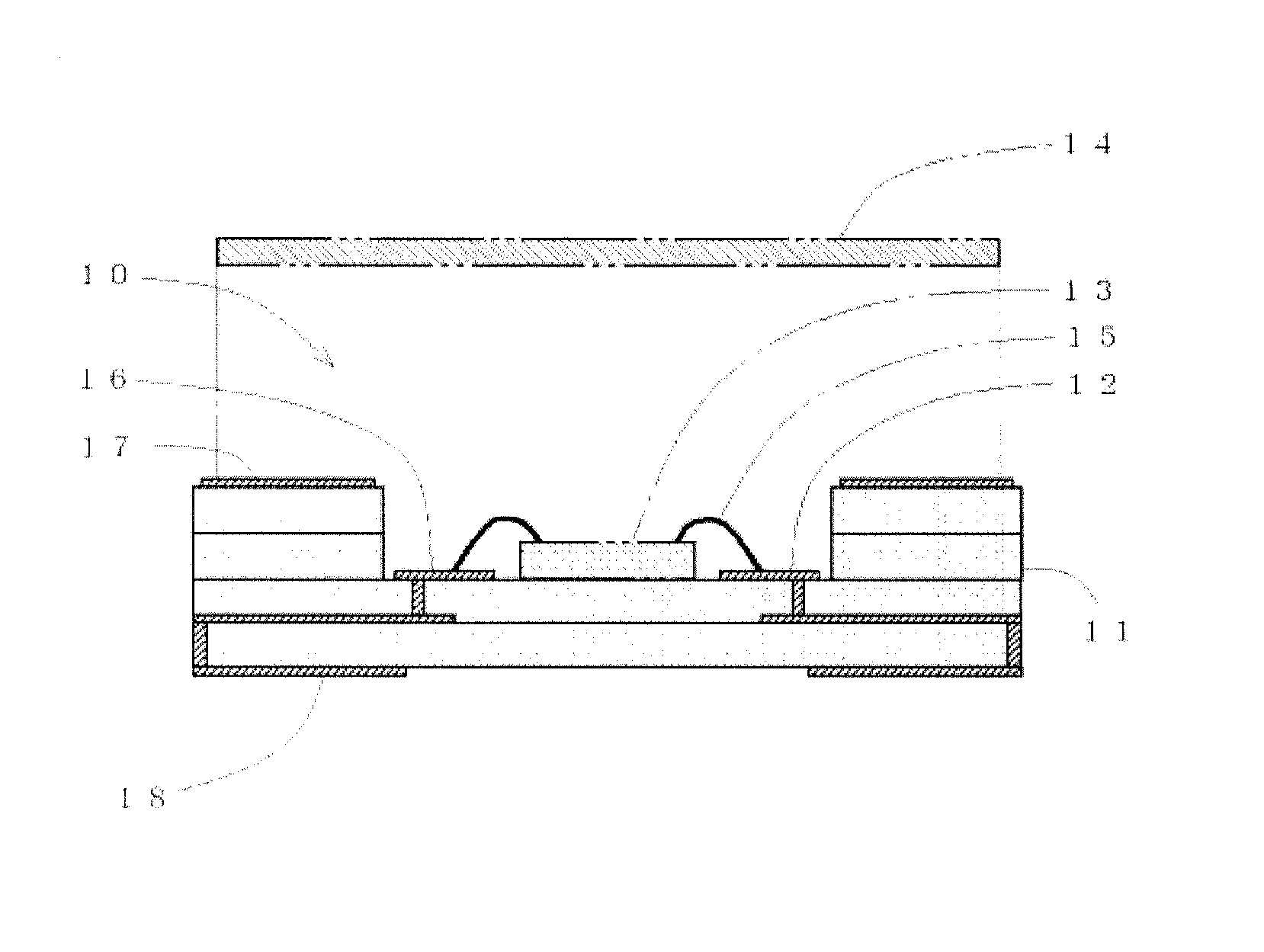
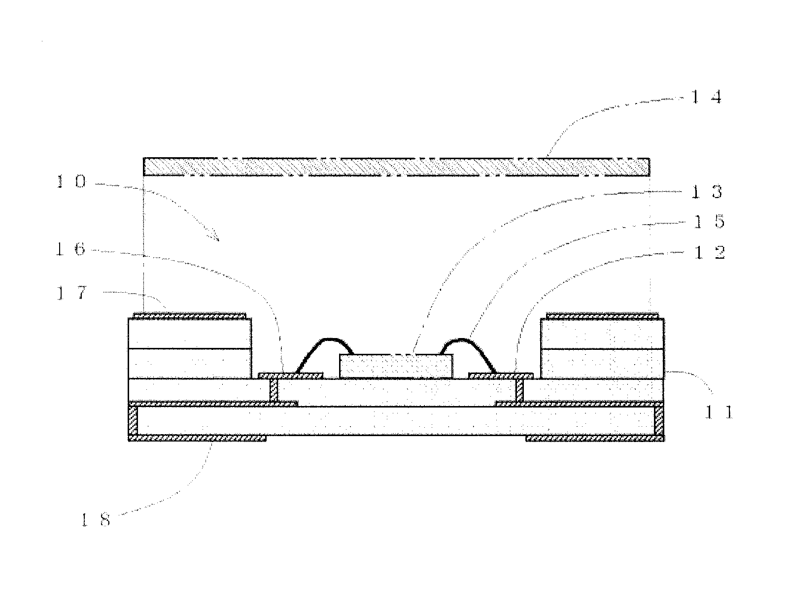
[0046]The inventor of the invention in the present application created samples of a ceramic substrate of alumina, and of alumina and zirconia partially stabilized by forming solid solution with yttria in component ratios of 95:5, 90:10, 80:20, and 70:30, and measured the bending strength of each ceramic substrate. The inventor also formed a metal layer on each of the ceramic substrates above with 94% by weight of tungsten, 3% by weight of molybdenum, and 3% by weight of a ceramic component, and measured the bond strength between the ceramic substrate and the metal layer. Table 1 shows the results thereof. As shown in Table 1, it is confirmed that if the partially stabilized zirconia by forming solid solution with ytttria is present at a rate of 10% by weight or greater, bending strength of 550 MPa or greater can be obtained. However, it is refer to the detail below confirmed that the bond strength between the ceramic substrate and the metal layer is under 10 MPa in ...

Example

Working Example 2

[0048]Next, the inventor of the present application produced ceramic substrates having a component percentage of 22% by weight for partially stabilized zirconia by forming solid solution with yttria, 0.5% by weight of magnesia, and a total content level of 0.5-6.0% by weight of a sintering agent having at least 1 type selected from among silica, calcia, and manganese oxide, with the remaining portion of alumina, and measured the bending strength of the ceramic substrates. In addition, the inventor formed a metal layer on each of the ceramic substrates above with 94% by weight of tungsten, 3% by weight of molybdenum, and 3% by weight of a ceramic component, and measured the bond strength between the ceramic substrate and the metal layer. Table 2 shows the results thereof. As shown in Table 2, it is confirmed that the working example having a content level of 1.5-4.5% by weight of the sintering agent having a combination of at least 1 type selected from among silica, ...

Example

[0052]However, when the inventor produced a sample of a conventional example (comparative example) having in the ceramic substrate 22% by weight of the partially stabilized zirconia and 7% by weight of the sintering agent of magnesia and silica and calcia, with the remaining portion of alumina, and measured the reflection rate of blue light with a wavelength of 450 nm under the same conditions, the reflection rate of the sample surface was 75%.

[0053]The thickness of the sample ceramic substrate in the working example and the conventional example used for measuring the reflection rate was 1 mm.

[0054]Therefore, the electronic component element housing package 10 according to the present embodiment has significantly greater reflectivity than the conventional example, and if the electronic component element mounted on the electronic component element housing package 10 is a light-emitting element, the ceramic substrate 10 itself can be made to function adequately as reflective material....


PUM

PropertyMeasurementUnit
Fractionaaaaaaaaaa
Percent by massaaaaaaaaaa

Abstract

An electronic component element housing package is produced by firing a ceramic substrate for housing an electronic component element and a metal layer for bonding to the ceramic substrate to form an electrical path, simultaneously in a reducing atmosphere. The ceramic substrate comprises alumina (Al2O3), a partially stabilized zirconia by forming solid solution with yttria (Y2O3) and a sintering agent. The sintering agent comprises magnesia (MgO), and at least 1 type selected from silica (SiO2), calcia (CaO), or manganese oxides (MnO, MnO2, Mn2O3, Mn3O4).

Description

CROSS-REFERENCE TO RELATED APPLICATIONS[0001]This application is a continuation application of International Patent Application No. PCT / JP2011 / 075109 filed on Oct. 31, 2011, which claims priority to Japanese Patent Application No. 2010-244975 filed on Nov. 1, 2010 in Japan.BACKGROUND OF INVENTION[0002]1. Field of the Invention[0003]The present invention relates to a layered ceramic electronic component element housing package for mounting and housing semiconductor elements, liquid crystal oscillators, and other electronic component elements, and more specifically, to a smaller and lower-profile electronic component element housing package capable of reducing the size and thickness of the ceramic substrate in order to house electronic component elements in a package and reduce the thickness and size of the device on which the elements are mounted.[0004]2. Background Art[0005]Conventionally, a plurality of ceramic green sheets was used in layered ceramic electronic component element h...

Claims


Application Information

Patent Timeline
IPC IPC(8): H05K5/02
CPCH01L23/057C04B2237/403H01L23/15H01L23/49822H01L23/49866H01L2924/09701H05K5/02H01L2224/32225H01L2224/73265H01L23/10C04B2237/343C04B2235/96C04B2235/3418H01L2224/48227C04B35/119C04B37/021C04B2235/3206C04B2235/3208C04B2235/3225C04B2235/3246C04B2235/3262C04B2235/3263C04B2235/3265C04B2235/3267H01L2924/00012B22F3/22B22F7/06C22C32/0031C22C32/0089C22C1/045H01L24/73
Inventor NAGAHIRO, MASANORI
Owner SUMITOMO METAL SMI ELECTRONICS DEVICES
Why Eureka
Try Eureka