Thin film transistor and display device
a thin film transistor and display device technology, applied in the direction of transistors, semiconductor devices, electrical equipment, etc., to achieve the effect of reducing the time to be taken for film formation, stabilizing electrical characteristics, and suppressing oxygen desorption
- Summary
- Abstract
- Description
- Claims
- Application Information
AI Technical Summary
Benefits of technology
Problems solved by technology
Method used
Image
Examples
first embodiment
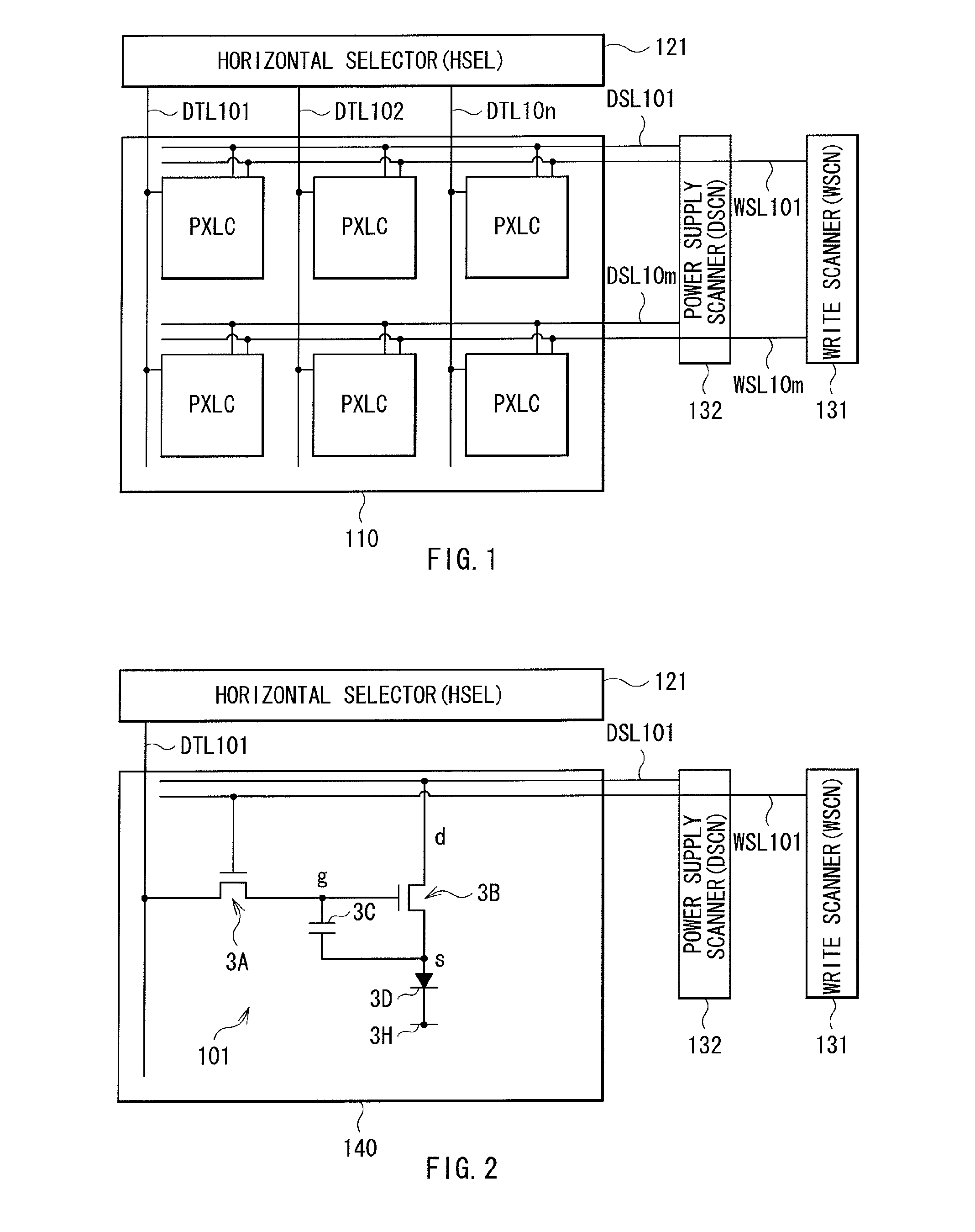
[0049]FIG. 1 is a diagram showing the configuration of a display device in a first embodiment of the invention. This display device is for use as an ultra-thin organic light-emitting color display device. For example, in this display device, a TFT substrate 1 that will be described later is provided thereon with a display region 110, in which pixels PXLC are arranged in a matrix. The pixels PXLC are each configured by any one of a plurality of organic light-emitting elements 10R, 10G, and 10B each being a display element and will be described later. This display region 110 is provided therearound with a horizontal selector (HSEL) 121 being a signal section, a write scanner (WSCN) 131 and a power supply scanner (DSCN) 132 each being a scanner section.
[0050]In the display region 110, signal lines DTL 101 to 10n are arranged in a column direction, and in a row direction, scan lines WSL 101 to 10m and power supply lines DSL 101 to 10mare arranged. At each intersection between the signal...
modified example 1
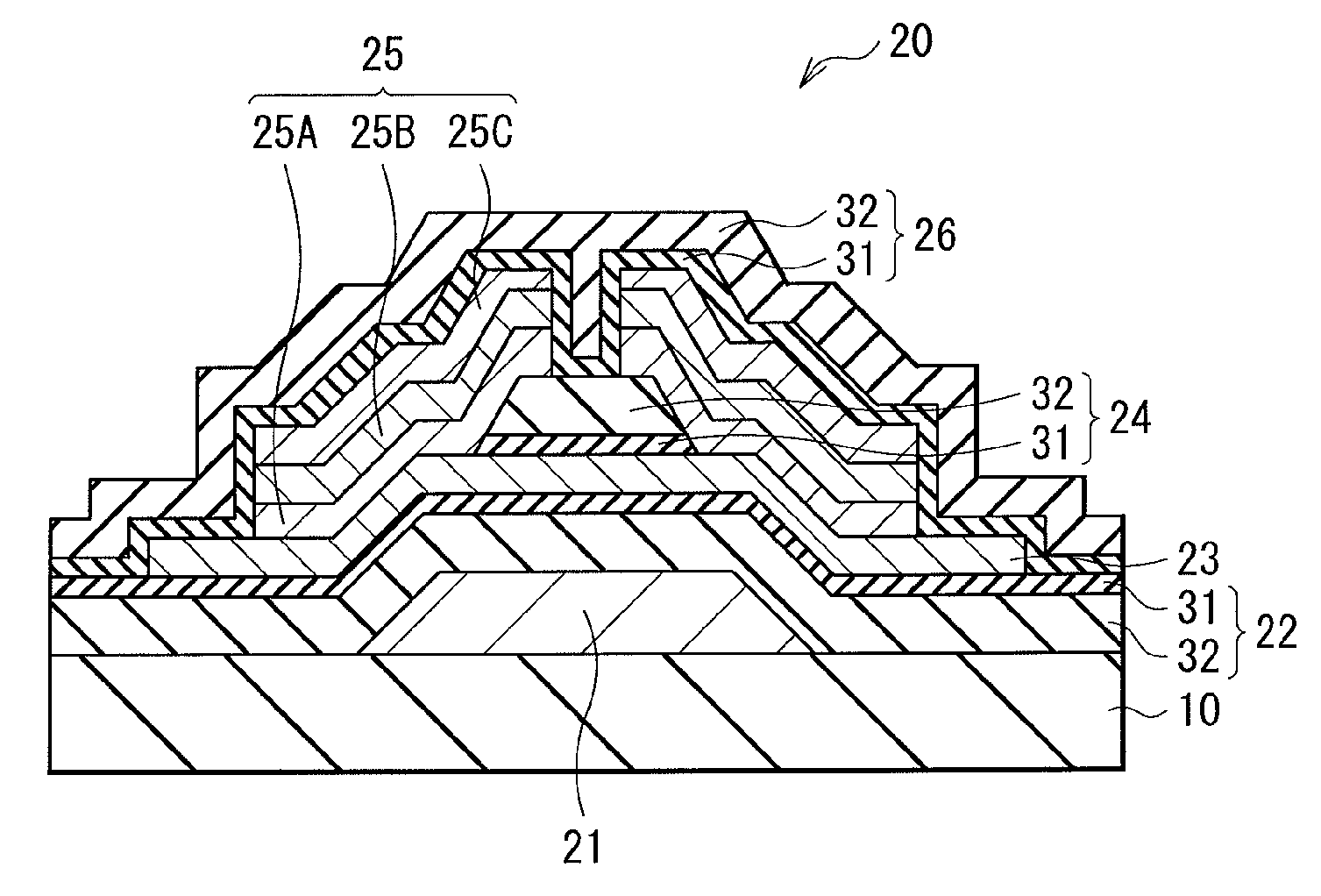
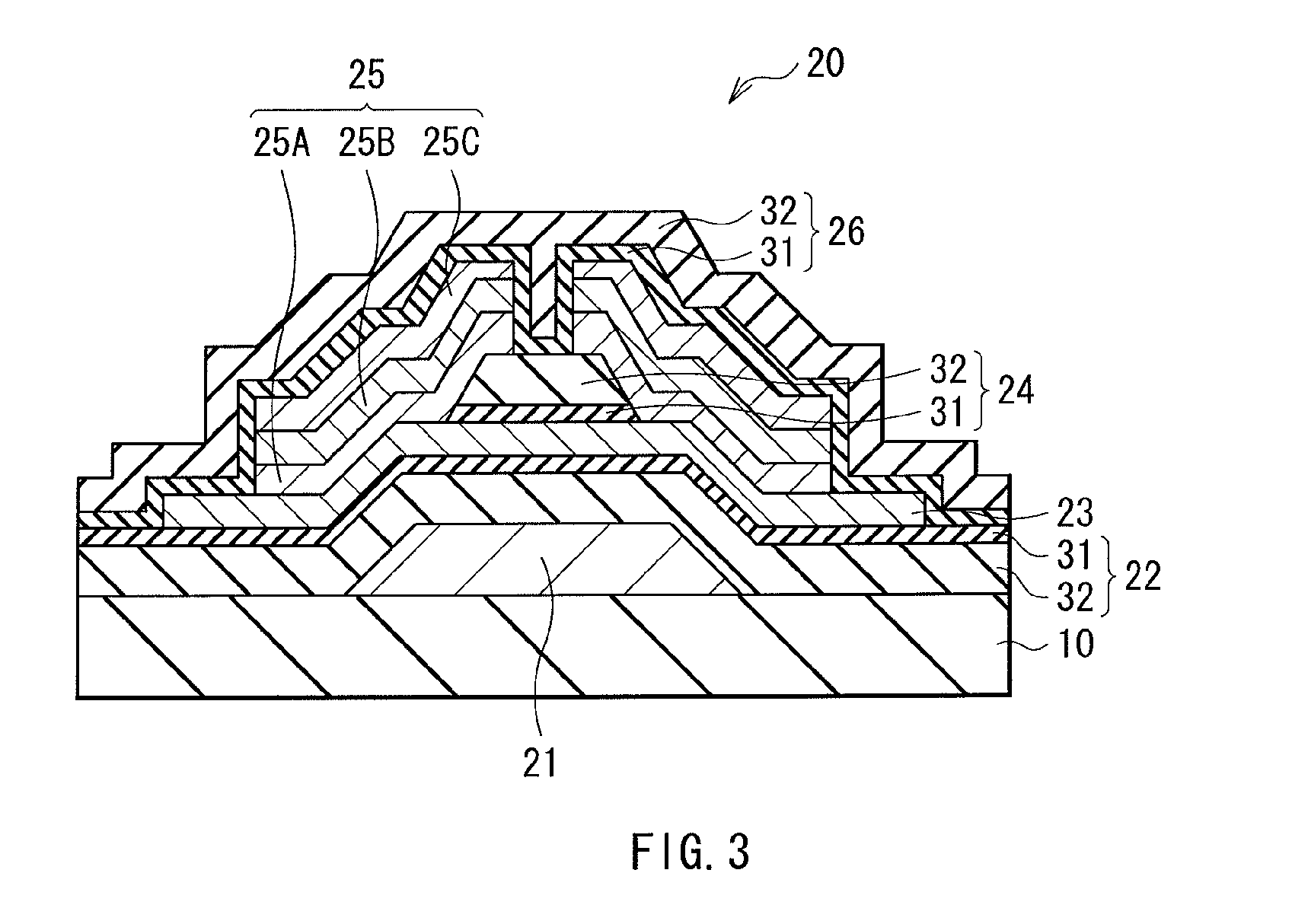
[0093]Note that, in the first embodiment described above, exemplified is the case in which the gate insulation film 22, the channel protection layer 24, and the passivation film 26 each have the laminate configuration including the first layer 31 made of aluminum oxide, and the second layer 32 made of an insulation material including silicon (Si). Alternatively, as shown in FIG. 7, only the gate insulation film 22 and the channel protection layer 24 may each have the laminate configuration including the first layer 31 made of aluminum oxide, and the second layer 32 made of an insulation material including silicon (Si). This configuration also enables to reduce the influence of gas such as oxygen by sandwiching the oxide semiconductor layer 23 between the first layer 31 of the gate insulation film 22 and the first layer 31 of the channel protection layer 24, thereby being able to increase the stability and reliability of the electrical characteristics of the TFT 20.
[0094]In this case...
modified example 2
[0095]Still alternatively, as shown in FIG. 8, only the gate insulation film 22 and the passivation film 26 may each have the laminate configuration including the first layer 31 made of aluminum oxide and the second layer 32 made of an insulation material including silicon (Si). This configuration also enables to reduce the influence of gas such as oxygen by sandwiching the oxide semiconductor layer 23 between the first layer 31 of the gate insulation film 22 and the first layer 31 of the passivation film 26, thereby being able to increase the stability and reliability of the electrical characteristics of the TFT 20.
[0096]In this case, the channel protection layer 24 has the thickness of about 300 nm, for example, and is configured by one or more of an aluminum oxide film, a silicon oxide film, a silicon nitride film, and a silicon oxynitride film.
PUM
 Abstract
Description
Claims
Application Information
 - R&D
- Intellectual Property
- Life Sciences
- Materials
- Tech Scout
- Unparalleled Data Quality
- Higher Quality Content
- 60% Fewer Hallucinations
Browse by: Latest US Patents, China's latest patents, Technical Efficacy Thesaurus, Application Domain, Technology Topic, Popular Technical Reports.
© 2025 PatSnap. All rights reserved.Legal|Privacy policy|Modern Slavery Act Transparency Statement|Sitemap|About US| Contact US: help@patsnap.com


