Active device and active device array substrate

a technology of active devices and array substrates, which is applied in the direction of semiconductor devices, basic electric elements, electrical apparatus, etc., can solve the problems of ineffective improvement of on-current technique, limited driving capacity of amorphous silicon thin film transistors in high-efficiency circuits, and inability to integrate peripheral high-speed driving circuits and control circuits, etc., to achieve the effect of improving on-curren

Inactive Publication Date: 2013-09-19
DONGGUAN MASSTOP LIQUID CRYSTAL DISPLAY +1
View PDF2 Cites 55 Cited by
  • Summary
  • Abstract
  • Description
  • Claims
  • Application Information

AI Technical Summary

Benefits of technology

[0008]An active device array substrate is provided, which utilizes a three-dimensional stack structure of a single gate electrode and dual channels to achieve circuit layout integration and improve ON-current.
[0009]An active device is provided, which utilizes a three-dimensional stack structure of a single gate electrode and dual channels to effectively improve ON-current.
[0018]Based on the above, in the active device of the active device array substrate of the disclosure, the single gate electrode is configured between the dual channels to increase the effective width of the device and thereby multiply the charge capacity of the thin film transistor. In addition, the two-dimensional circuit layout is integrated in a three-dimensional way by vertically configuring the gate electrode, dual channels, dual sources, and dual drains on the substrate, so as to further reduce the layout area of the circuit layout and effectively improve pixel aperture ratio, or effectively reduce the space for the circuit layout. Accordingly, the difficulty of maintaining the driving capacity and aperture ratio of the thin film transistor at the same time, which occurs in the conventional large-sized devices, is overcome.

Problems solved by technology

However, the application of amorphous silicon thin film transistor (a-Si TFT) in high-efficiency circuits is limited by its driving capacity.
As a result, amorphous silicon thin film transistor cannot integrate the peripheral high-speed driving circuit and control circuit.
However, the conventional technique cannot effectively improve the ON-current due to the limitations of the manufacturing process.
However, this technique causes reduction of the pixel aperture ratio and decreases the overall brightness of the TFT LCDs, and threshold voltage shift may easily occur.
The back channel may easily cause damage to the channel layer during the manufacturing process.
Therefore, the dual gate structure faces the problem that the current may be attenuated easily and the improvement of the ON-current is limited.
Moreover, this technique cannot integrate the circuit layout to reduce the device area of TFT, improve pixel aperture ratio, and maintain high brightness.

Method used


Image

  • Active device and active device array substrate
  • Active device and active device array substrate
  • Active device and active device array substrate

Examples


first embodiment

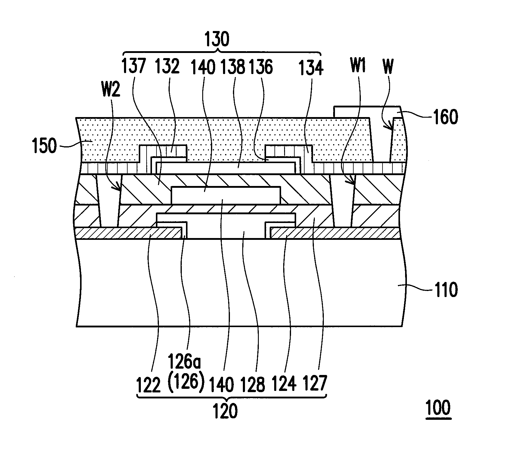
[0031]FIG. 1 is a schematic cross-sectional view of an active device array substrate according to the disclosure. Referring to FIG. 1, an active device array substrate 100 of this embodiment includes a substrate 110, a first transistor 120, a second transistor 130, a common gate electrode 140, a protective layer 150, and a pixel electrode 160. The first transistor 120 is disposed on the substrate 110, wherein the first transistor 120 includes a first channel layer 128. The second transistor 130 is stacked on the first transistor 120, wherein the second transistor 130 includes a second channel layer 138. The first transistor 120 and the second transistor 130 share the common gate electrode 140, and the common gate electrode 140 is disposed between the first channel layer 128 and the second channel layer 138.

[0032]More specifically, the first transistor 120 includes a first source 122, a first drain 124, a first doped amorphous silicon layer 126, and a first gate insulating layer 127....

third embodiment

[0050]FIG. 6A is a schematic top view of an active device in an active device array substrate according to the disclosure, which is an improvement to the layout space of the active device in the conventional active device array substrate of FIG. 5. FIG. 6B is a schematic cross-sectional view taken along the line A-A′ in FIG. 6A. Referring to FIGS. 6A and 6B, identical elements are indicated by the same reference numbers. According to the disclosure, the first transistor 320 and the second transistor 330 in the active device 300 of FIG. 5 are stacked in the form of a three-dimensional structure, and the first drain 224 of the first transistor 320 and the second drain 134 of the second transistor 330 are electrically connected through the first contact via W1, so as to connect the two transistor 320 and 330 in series. In addition, an opening W is formed in the protective layer 150 on the second drain 134 of the second transistor 330, and the signal outputting trace 380 is electrically...


PUM


Abstract

An active device and an active device array substrate are provided, wherein the active device array substrate includes a substrate and a plurality of active devices being located on the substrate, and at least one of the active devices includes a first thin film transistor and a second thin film transistor. The first thin film transistor is located on the substrate and has a first channel layer. The second thin film transistor stacks on the first thin film transistor, wherein the second thin film transistor has a second channel layer. The first thin film transistor and the second thin film transistor share a common gate electrode and the common gate electrode is located between the first channel layer and the second channel layer.

Description

CROSS-REFERENCE TO RELATED APPLICATION[0001]This application claims the priority benefit of Taiwan application serial no. 101108652, filed on Mar. 14, 2012. The entirety of the above-mentioned patent application is hereby incorporated by reference herein and made a part of this specification.BACKGROUND OF THE INVENTION[0002]1. Technical Field[0003]The invention relates to an active device and an active device array substrate, and more particularly, relates to a dual-channel active device and a dual-channel active device array substrate.[0004]2. Description of Related Art[0005]As electronic technology develops, the thin film transistor liquid crystal display (TFT LCD) having superior properties such as high definition, great space utilization, low power consumption and no radiation gradually becomes a mainstream in the display market.[0006]To satisfy the demand for large-sized and high-resolution TFT LCDs, the thin film transistor is required to have high-mobility carriers, so as to ...

Claims


Application Information

Patent Timeline
Patent Type & Authority Applications(United States)
IPC IPC(8): H01L27/12
CPCH01L27/1222H01L27/1225H01L27/1251
Inventor YEH, CHENG-YENCHEN, YU-TING
Owner DONGGUAN MASSTOP LIQUID CRYSTAL DISPLAY
Why Eureka
Try Eureka