Breakdown voltage multiplying integration scheme

a voltage multiplying and integration scheme technology, applied in the field of electrical and electronic arts, can solve the problems of large capacitance values that cannot be implemented by solids, the inability to implement these conventional voltage multiplying circuits as integrated circuits, and the impracticality of large area consumed by high-voltage capacitors for typical applications

Inactive Publication Date: 2013-09-19
ALSEPHINA INNOVATIONS INC
View PDF6 Cites 38 Cited by
  • Summary
  • Abstract
  • Description
  • Claims
  • Application Information

AI Technical Summary

Benefits of technology

[0004]Principles of the invention provide techniques for a breakdown voltage multiplying integration scheme. In one aspect, an exemplary circuit includes a first field effect transistor having a gate, a first drain-source terminal, and a second drain-source terminal. The first field effect transistor includes one of an n-channel transistor and a p-channel transistor. Also included is a second field effect transistor...

Problems solved by technology

For operation under large DC current loads, conventional voltage multiplying circuits, such as the Cockcroft-Walton (CW) AC-to-DC converter shown in FIG. 11, require large capacitance values that cannot be implemented by solid-state devices unless impractically large device areas are used.
As a result of the required large capacitor values, desp...

Method used


Image

  • Breakdown voltage multiplying integration scheme
  • Breakdown voltage multiplying integration scheme
  • Breakdown voltage multiplying integration scheme

Examples


Embodiment Construction

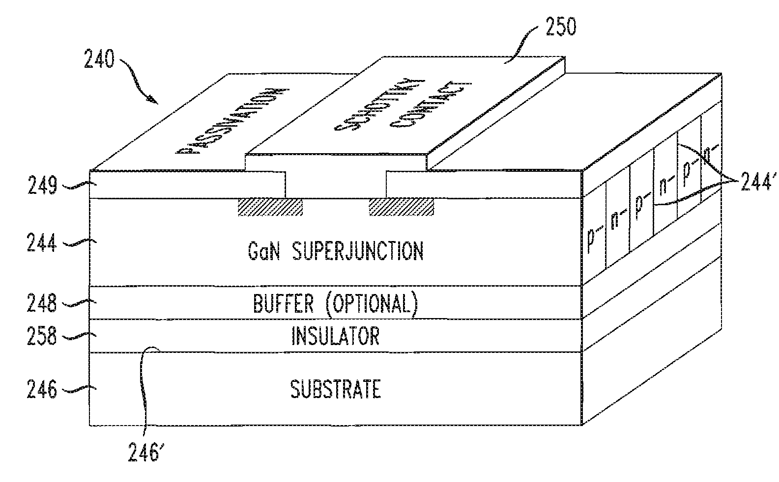
[0030]As noted above, for operation under large DC current loads, conventional voltage multiplying circuits, such as the CW AC-to-DC converter, require large capacitance values that cannot be implemented by solid-state devices unless very large device areas are used. For example, assume 10 nF metal-insulator-metal capacitors fabricated with 2 μm silicon dielectric layers having a large area of 6 cm2, allowing a breakdown voltage of 2.5 KV. Further, assume GaN Schottky diodes with the same breakdown voltages of 2.5 KV. Under such assumptions, voltage multiplication from 2.5 KV (peak-to-peak) to 5 KV (using a 2 stage multiplier) and 10 KV (using a 4 stage multiplier) is expected, under 75 KHz and 500 KHz operation, respectively. However, the capacitor area of 6 cm2 is very large and impractical for typical applications. Such large areas are needed because a sufficiently thick dielectric material is needed to sustain the high voltages, therefore limiting the value of capacitance per ar...


PUM


Abstract

A circuit includes a first field effect transistor having a gate, a first drain-source terminal, and a second drain-source terminal; and a second field effect transistor having a gate, a first drain-source terminal, and a second drain-source terminal. The second field effect transistor and the first field effect transistor are of the same type, i.e., both n-channel transistors or both p-channel transistors. The second drain-source terminal of the first field effect transistor is coupled to the first drain-source terminal of the second field effect transistor; and the gate of the second field effect transistor is coupled to the first drain-source terminal of the second field effect transistor. The resulting three-terminal device can be substituted for a single field effect transistor that would otherwise suffer breakdown under proposed operating conditions.

Description

FIELD OF THE INVENTION[0001]The present invention relates to the electrical and electronic arts, and, more particularly, to electronic circuitry and the like.BACKGROUND OF THE INVENTION[0002]For operation under large DC current loads, conventional voltage multiplying circuits, such as the Cockcroft-Walton (CW) AC-to-DC converter shown in FIG. 11, require large capacitance values that cannot be implemented by solid-state devices unless impractically large device areas are used. The CW is made up of a voltage multiplier ladder network of capacitors 1102, 1104, 1106, 1108 and diodes 1110, 1112, 1114, 1116 to generate high voltages. The CW is attached to an AC input voltage 1118. At the time when the AC input voltage 1118 reaches its negative pole the leftmost diode 1110 is allowing current to flow from the ground into the first capacitor 1102, charging it up. When the same AC signal reverses polarity, current flows through the second diode 1112 charging up the second capacitor with bot...

Claims


Application Information

Patent Timeline
IPC IPC(8): H01L27/088G06F17/50
CPCH01L27/088H01L27/0605H01L21/8252G06F17/5063H01L29/872H01L29/205H01L29/402H01L29/66462H01L21/6835H01L2221/68363H01L29/0634H01L29/2003H01L29/7786G06F30/36G06F30/30G06F30/323G06F30/373H01L27/095
Inventor BEDELL, STEPHEN W.HEKMATSHOARTABARI, BAHMANSADANA, DEVENDRA K.SHAHIDI, GHAVAM G.SHAHRJERDI, DAVOOD
Owner ALSEPHINA INNOVATIONS INC
Why Eureka
Try Eureka