Thin film transistor and manufacturing method thereof

a thin film transistor and manufacturing method technology, applied in the direction of transistors, semiconductor devices, electrical apparatus, etc., can solve the problems of shortening the life of tft, affecting the oxide channel layer during the manufacturing process, and deteriorating the element characteristic of tft, so as to achieve the desired electro-optical characteristic and stability

Inactive Publication Date: 2013-10-03
DONGGUAN MASSTOP LIQUID CRYSTAL DISPLAY +1
View PDF9 Cites 36 Cited by
  • Summary
  • Abstract
  • Description
  • Claims
  • Application Information

AI Technical Summary

Benefits of technology

[0008]The invention provides a thin film transistor having desirable electro-optica

Problems solved by technology

In addition, the photo current generated by the oxide channel layer under the UV light irradiation would shorten the lifetime of the TFT and deteriorate the element characteristic of the TFT.
A

Method used


Image

  • Thin film transistor and manufacturing method thereof
  • Thin film transistor and manufacturing method thereof
  • Thin film transistor and manufacturing method thereof

Examples


Embodiment Construction

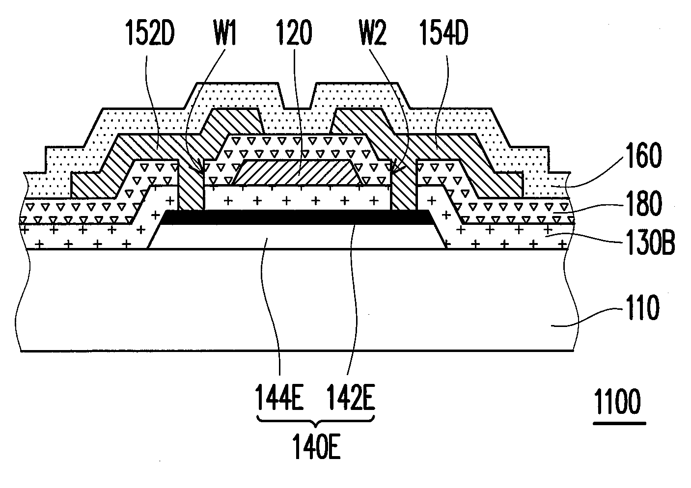
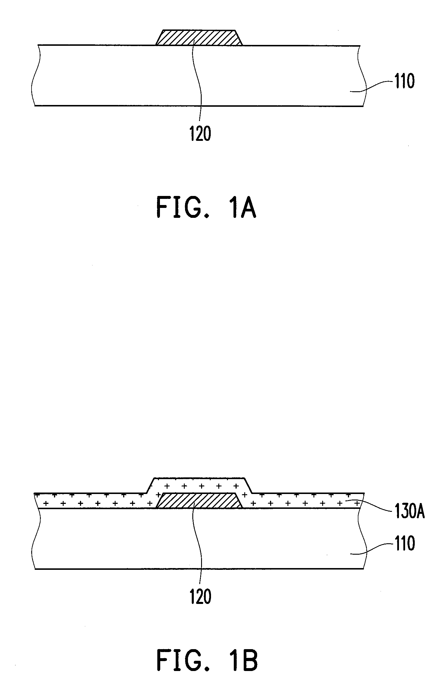
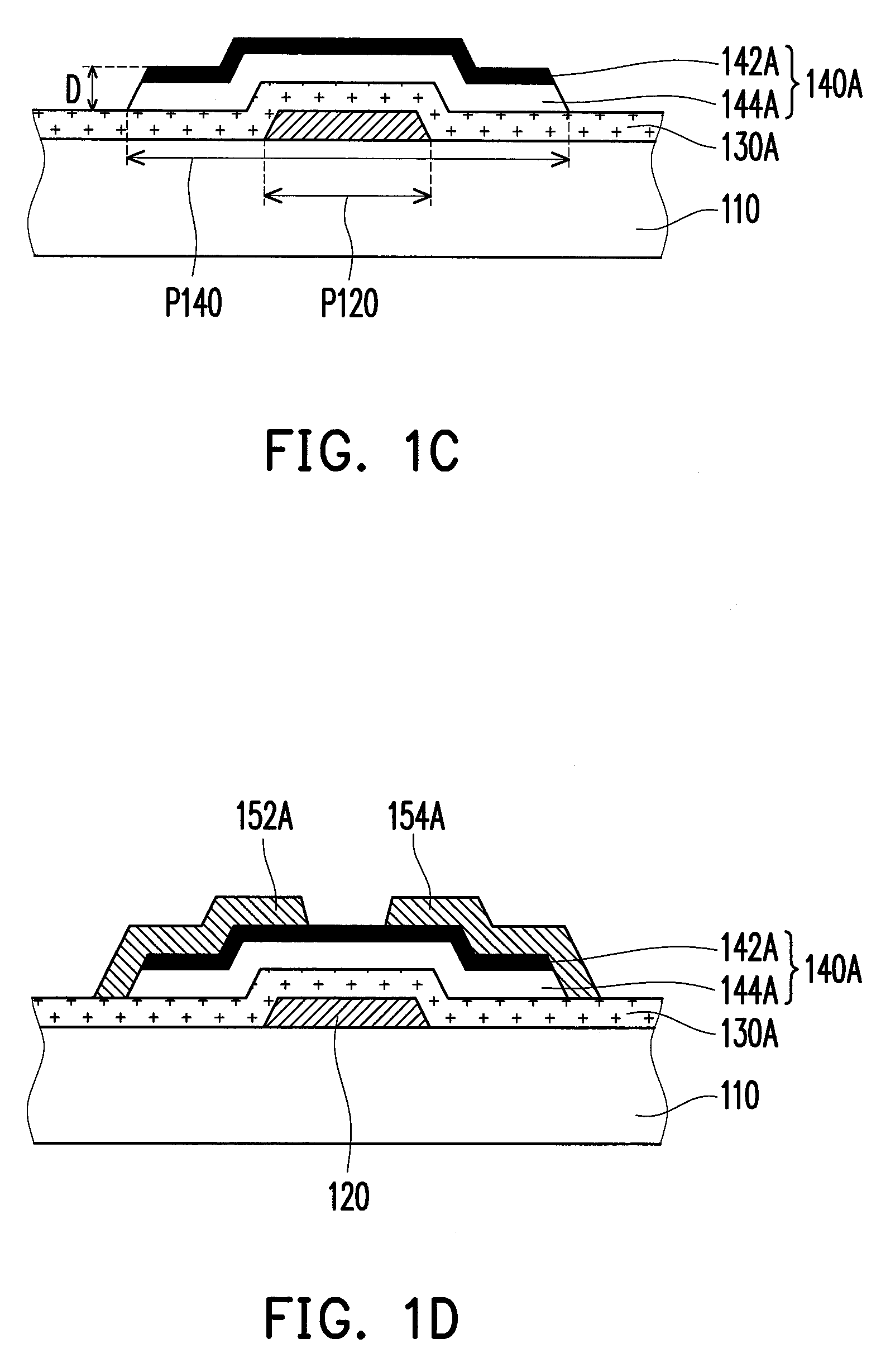
[0033]FIG. 1A to FIG. 1F are schematic views illustrating a process of manufacturing a TFT according to an embodiment of the invention.

[0034]Referring to FIG. 1A, a substrate 110 is provided and a gate 120 is formed on the substrate 110, wherein the gate 120 can be formed by a stack of metal layers or a single metal layer and the material of the gate 120 can be Al, Cu or other metals having high conductivity. It is noted that according to the requirement, the gate 120 can be made by non-metal conductive material such as Indium Tin Oxide (ITO).

[0035]Referring to FIG. 1B, a gate insulation layer 130A is formed on the substrate 110, so as to cover the gate 120. The material of the gate insulation layer 130A includes an inorganic material (e.g. silicon oxide, silicon nitride, silicon oxynitride, silicon aluminum oxide, or a stacked layer of the above materials), an organic material, or a combination of the above. It is noted that the embodiment is not limited thereto and any material ha...


PUM


Abstract

A thin film transistor and a manufacturing method thereof are provided. The thin film transistor includes a gate, an oxide channel layer, a gate insulating layer, a source, a drain and a dielectric layer. The gate is disposed on a substrate. The oxide channel layer, disposed on the substrate, is stacked with the gate. A material of the oxide channel layer includes a metal element. The metal element content shows a gradient distribution along a thickness direction of the oxide channel layer. The gate insulation layer is disposed between the gate and the oxide channel layer. The source and the drain are disposed in parallel to each other, and connected to the oxide channel layer. Sides of the source and the drain, facing away from the substrate, are covered by the dielectric layer.

Description

CROSS-REFERENCE TO RELATED APPLICATION[0001]This application claims the priority benefit of Taiwan application serial no. 101110788, filed on Mar. 28, 2012. The entirety of the above-mentioned patent application is hereby incorporated by reference herein and made a part of this specification.BACKGROUND OF THE DISCLOSURE[0002]1. Field of the Disclosure[0003]The invention relates to a semiconductor device and a manufacturing method thereof, and more particularly to a thin film transistor and a manufacturing method thereof.[0004]2. Description of Related Art[0005]With the proceeding improvement of the electronic technology, thin film transistor liquid crystal displays (TFT-LCD) have recently become a mainstream product in the display market due to the advantages such as high image quality, great space efficiency, low power consumption and no radiation.[0006]Owing to the requirement of the TFT-LCD on large area and high resolution, the TFT therein needs have high carrier mobility so as ...

Claims


Application Information

Patent Timeline
IPC IPC(8): H01L29/786H01L29/66
CPCH01L29/78693H01L29/78696H01L29/7869H01L29/66765
Inventor CHANG, HUI-YUYU, MING-CHANGCHIOU, CHANG-CHINGHAN, HSI-RONG
Owner DONGGUAN MASSTOP LIQUID CRYSTAL DISPLAY
Why Eureka
Try Eureka