Small-Grain Three-Dimensional Memory

a three-dimensional memory and small-grain technology, applied in the field of integrated circuits, can solve the problems of limited storage density, large current fluctuation, poor performance of prior-art 3d-m, etc., and achieve the effect of improving the performance of small-pitch 3d-m, increasing the storage density of small-pitch 3d-m, and reducing the read/write error rate of small-pitch 3d-m

Active Publication Date: 2013-10-03
CHENGDU HAICUN IP TECH +1
View PDF4 Cites 14 Cited by
  • Summary
  • Abstract
  • Description
  • Claims
  • Application Information

AI Technical Summary

Benefits of technology

[0009]It is a principle object of the present invention to improve the performance of the small-pitch 3D-M.
[0010]It is a further object of the present invention to increase the storage density of the small-pitch 3D-M.
[0011]It is a further object of the present invention to reduce the read/write error rate of the small-pitch 3D-M.
[0012]It is a further object of the present invention to improve the consistency of memory cells in a small-pitch 3D-M.
[0013]In accordance with these and other objects of the present invention, the present invention discloses a small-grain 3D-M (3D-MSG). It makes further improvement to the small-pitch 3D-M (3D-MSP).
[0014]In order to limit the performance variation of the thin-film diode in a 3D-M, the present invention discloses a small-grain 3D-M (3D-MSG). The 3D-MSG is particularly suitable for the 3D-M whose critical dimension is scaled to 40 nm or below. Its thin-film diode is a s

Problems solved by technology

This leads to unacceptable read/write error rate.
Furthermore, a large current fluctuation becomes more troublesome when multi-bit-per-cell is employed to increase the st

Method used


Image

  • Small-Grain Three-Dimensional Memory
  • Small-Grain Three-Dimensional Memory
  • Small-Grain Three-Dimensional Memory

Examples


Embodiment Construction

[0022]Those of ordinary skills in the art will realize that the following description of the present invention is illustrative only and is not intended to be in any way limiting. Other embodiments of the invention will readily suggest themselves to such skilled persons from an examination of the within disclosure.

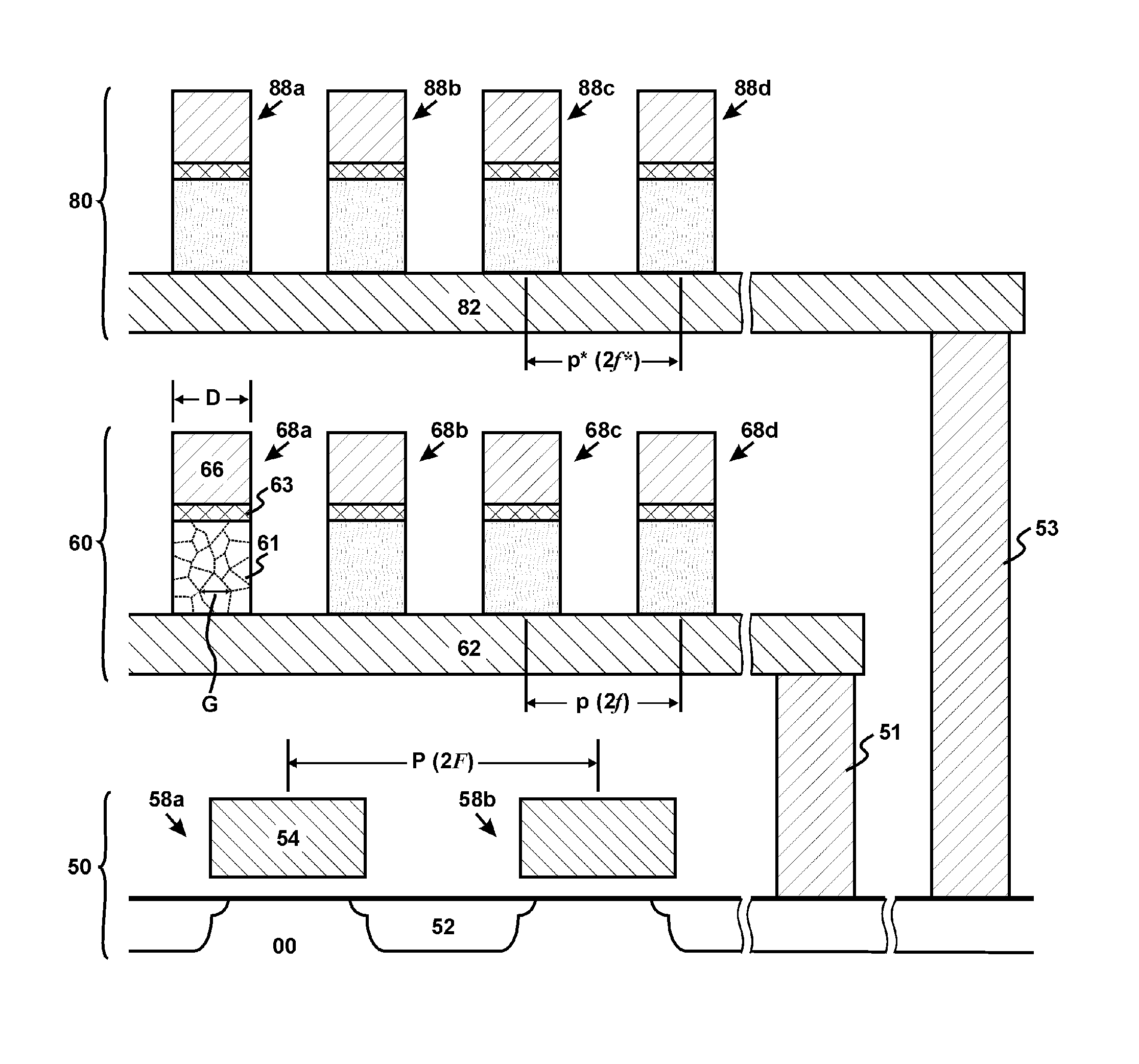
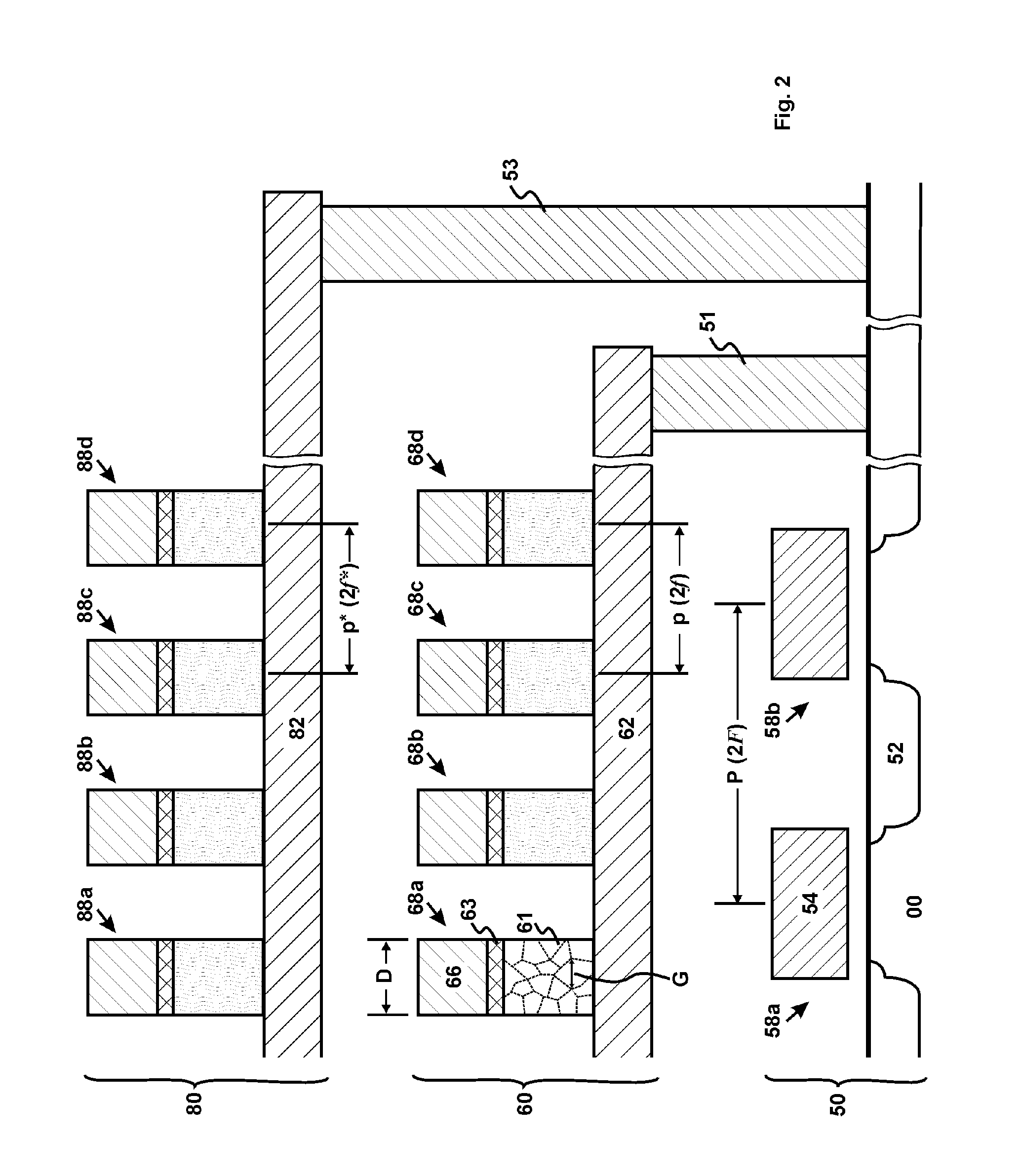
[0023]Referring now to FIG. 2, a preferred small-grain 3D-M (3D-MSG) is disclosed. It comprises a substrate level 50 and at least two memory levels 60, 80. The substrate level 50 comprises a plurality of functional transistors 58a, 58b. Formed in the substrate 00, these transistors are single-crystalline transistors. Here, “functional transistors”, unlike “dummy transistors”, perform certain chip functions, e.g. supporting function (e.g. a peripheral circuit for the 3D-M) and / or storage function (e.g. a transistor-based memory, such as a RAM array or a ROM array). The transistor-gate pitch P is the center-to-center distance between the poly gates of adjacent transistors 58a...


PUM


Abstract

The present invention discloses a small-grain three-dimensional memory (3D-MSG). Each of its memory cells comprises a thin-film diode with critical dimension no larger than 40 nm. The thin-film diode comprises at least a small-grain material, whose grain size G is substantially smaller than the diode size D. The small-grain material is preferably a nano-crystalline material or an amorphous material. The critical dimension f of the small-grain diode is smaller than the critical dimension F of the single-crystalline transistor.

Description

CROSS-REFERENCE TO RELATED APPLICATIONS[0001]This application claims foreign priority of a Chinese Patent Application Ser. No. 201210089545.5, “Small-Grain Three-Dimensional Memory”, filed in People's Republic of China on Mar. 30, 2012.BACKGROUND[0002]1. Technical Field of the Invention[0003]The present invention relates to the field of integrated circuit, and more particularly to diode-based monolithic three-dimensional semiconductor memory.[0004]2. Prior Arts[0005]Three-dimensional memory (3D-M) is a monolithic semiconductor memory. It comprises a plurality of vertically stacked memory levels. As illustrated in FIG. 1, a 3D-M comprises at least a substrate level 30 and a memory level 40. The substrate level 30 comprises a plurality of transistors (38a . . . ). Formed in a single-crystalline semiconductor substrate 00, these transistors are single-crystalline transistors. Each transistor further includes a gate 34 and a source / drain 32. The memory level 40 comprises a plurality of ...

Claims


Application Information

Patent Timeline
IPC IPC(8): G11C5/02G11C17/16
CPCG11C5/02G11C17/16G11C11/5692G11C13/0004G11C2213/73G11C13/0011G11C17/10G11C2213/71G11C13/0007
Inventor ZHANG, GUOBIAO
Owner CHENGDU HAICUN IP TECH
Why Eureka
Try Eureka