Infrared absorbing glass wafer and method for producing same

a technology of infrared absorbing glass and glass wafers, which is applied in the field of glass wafers, can solve the problems of unfavorable cost-efficient manufacturing, color and brightness distortion, annoying ghost images in the optical system, etc., and achieve the effect of low curvatur

Active Publication Date: 2013-10-10
SCHOTT AG
View PDF2 Cites 9 Cited by
  • Summary
  • Abstract
  • Description
  • Claims
  • Application Information

AI Technical Summary

Benefits of technology

[0023]According to the thicknesses indicated above, for manufacturing the wafer the glass is thinned by at least a factor of 4.5 by polishing, or by grinding followed by polishing. The method may seem to be complicated at first glance, but in this way a high plane-parallelism of the glass wafer and especially a low curvature (also referred to as “warpage”) can be achieved.

Problems solved by technology

However, infrared light that reaches the chip results in undesirable color and brightness distortions.
Since the interference filter generally still exhibits a residual transmission at least in the near infrared range, very annoying ghost images may occur in the optical system due to multiple reflections.
However, heretofore, their cost-efficient manufacturing is not the only advantage of interference filters when compared to filter glasses.
However, a problem usually arising with thin glasses is a ripple of the glass surface and the uniformity of the glass thickness.

Method used


Image

  • Infrared absorbing glass wafer and method for producing same
  • Infrared absorbing glass wafer and method for producing same
  • Infrared absorbing glass wafer and method for producing same

Examples


Embodiment Construction

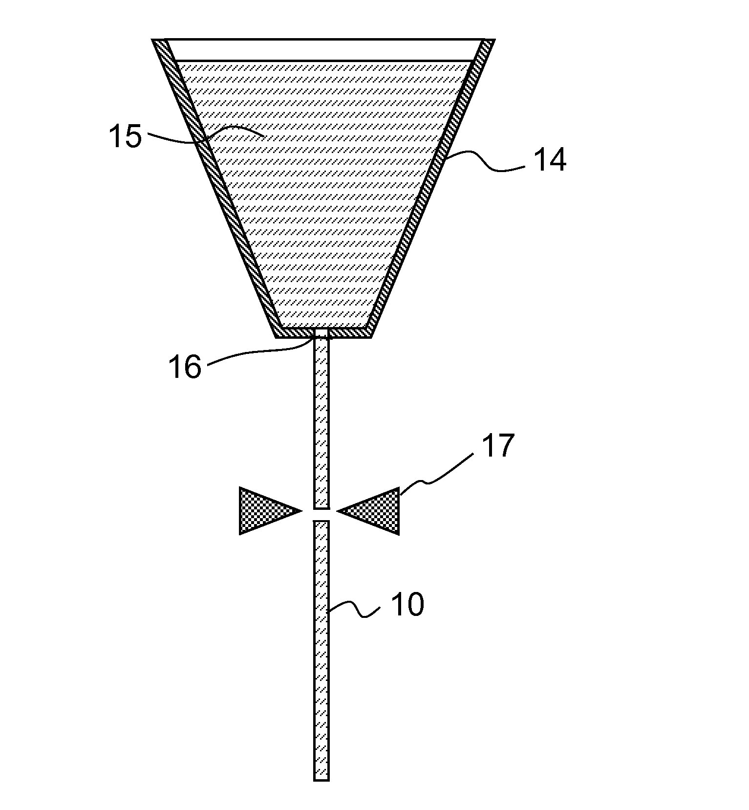
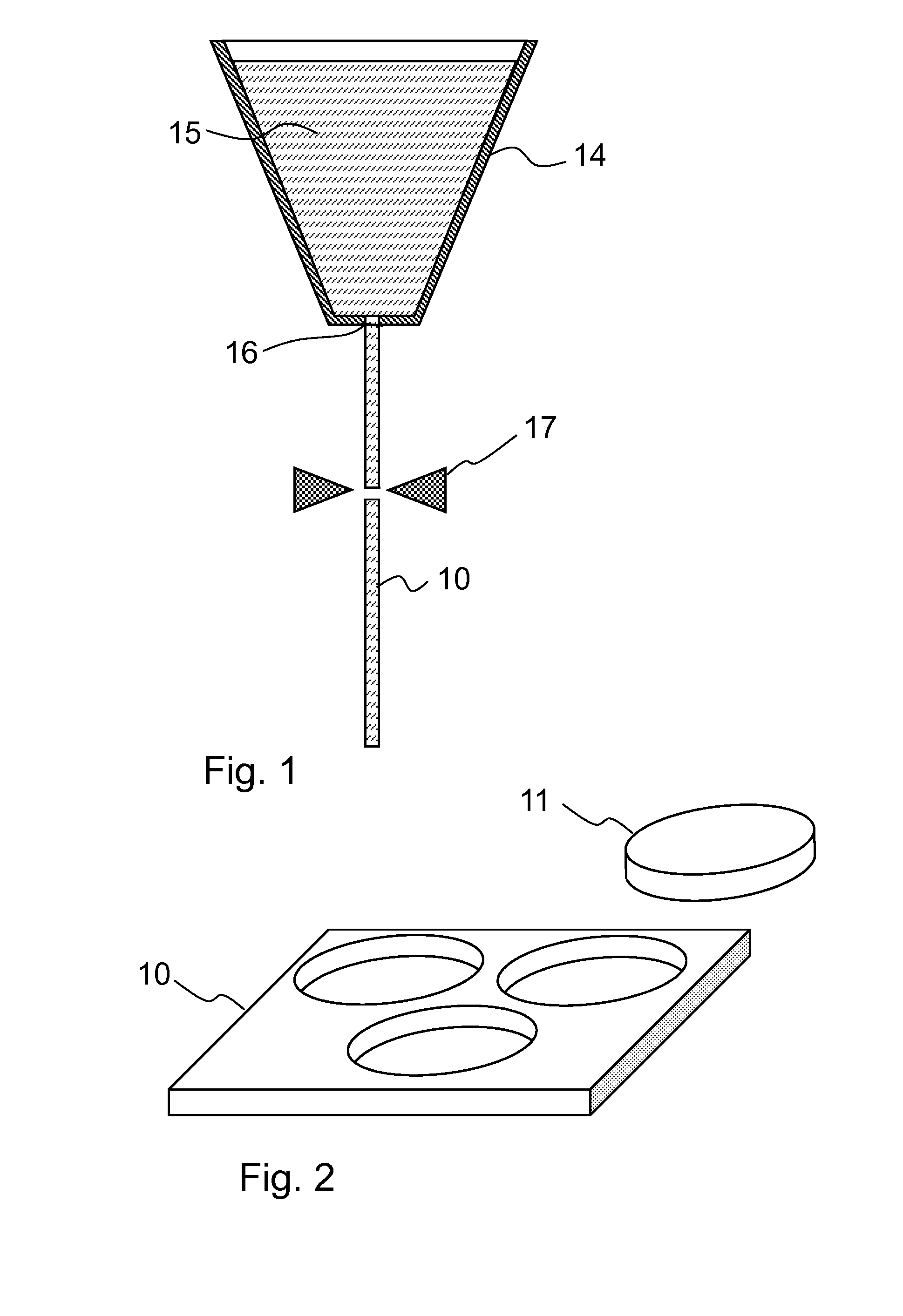
[0031]Referring to FIGS. 1, 2, and 3, the manufacturing of a glass wafer according to the invention will be described schematically. First, the molten glass from which the glass sheet is produced, is prepared by a preferably continuous melting process. FIG. 1 shows a crucible 14 having a slotted nozzle at its bottom. The crucible may be formed by the melting trough itself, or the fluorophosphate or phosphate glass melt 15 produced in the melting trough is filled into crucible 14. A strip of glass exiting from slotted nozzle 16 is separated into individual glass sheets 10 using a cutting tool 17. Accordingly, in this exemplary embodiment the glass sheets are manufactured in a so-called downdraw process. Alternatively, however, other processes are likewise possible, such as a float process or overflow fusion process.

[0032]The thus produced glass sheets 10 have a thickness of at least 1.8 millimeters, preferably from 1.8 to 3.2 millimeters, more preferably a thickness in a range from 2...


PUM

PropertyMeasurementUnit
thicknessaaaaaaaaaa
diameteraaaaaaaaaa
lengthaaaaaaaaaa

Abstract

A glass wafer is provided that is made of a copper ions containing phosphate or fluorophosphate glass. The glass wafer has a diameter greater than 15 centimeters and a thickness of less than 0.4 millimeters. The glass wafer has two plane-parallel surfaces at least one of which is polished.

Description

CROSS REFERENCE TO RELATED APPLICATIONS[0001]This application claims benefit under 35 U.S.C. §119(a) of German Patent Application No. De 10 2012 103 077.4, filed Apr. 10, 2012, the entire contents of which are incorporated herein by reference.BACKGROUND OF THE INVENTION[0002]1. Field of the Invention[0003]The invention generally relates to glass wafers. More particularly, the invention relates to glass wafers made of infrared absorbing glasses.[0004]2. Description of Related Art[0005]As is known, camera chips typically have the property that the pixels of the chip are sensitive also in the infrared spectral range. Moreover, the optical system of camera modules whose optical components are made from standard glasses or plastic materials generally exhibit a certain amount of infrared transmission. However, infrared light that reaches the chip results in undesirable color and brightness distortions.[0006]For this reason, camera modules are typically equipped with infrared filters. The ...

Claims


Application Information

Patent Timeline
Patent Type & Authority Applications(United States)
IPC IPC(8): G02B5/22H01L31/0216G02B5/20G03B11/00
CPCG02B5/208H01L27/146G02B5/226H01L31/0216C03C3/00H01L27/14621C03C3/17C03C3/247C03C4/082H01L27/14G02B5/28G02B5/20
Inventor SCHREDER, BIANCAFREUND, JOCHENWOELFEL, UTEMARTINBAUR, CHRISTOPHEREICHESL, STEFFENCLEMENT, MARC
Owner SCHOTT AG
Why Eureka
Try Eureka