Power droop reduction via clock-gating for at-speed scan testing

a technology of clock gating and at-speed scan, which is applied in the direction of pulse generators, pulse techniques, instruments, etc., can solve the problems of sudden demand for a large amount of current from power droop on the power grid of the device, so as to reduce the power droop during at-speed testing of the device, reduce the test time, and increase the test yield

Inactive Publication Date: 2013-10-17
NVIDIA CORP
View PDF7 Cites 17 Cited by
  • Summary
  • Abstract
  • Description
  • Claims
  • Application Information

AI Technical Summary

Benefits of technology

[0011]One advantage of the disclosed technique is that power droop during at-speed testing of a device is reduced without significantly increasing the quantity of ATPG test vectors, resulting in greater test yields and lower test times.

Problems solved by technology

A rapid shift from the scan-load (quiescent) phase to the capture (active) phase causes a sudden demand for a large amount of current from the power grid of the device.
As a result, the power grid may temporarily experience an inductive reaction to the sudden demand for current.
The inductive reaction, in turn, causes a power droop on the power grid of the device.
Such a power droop may cause the device to fail the at-speed test or to operate at a slower speed during the test.
Such a failure or reduction in operational speed, however, may amount to a false negative.
In other words, the failure of the device during at-speed testing does not mean the device fails to meet the requirements for normal operation.
One problem with this approach is testing the device at a lower speed increases test times. Another potential solution is to switch fewer transistors at a time during automated testing.
One problem with this approach is that a higher number of test vectors is required to test the device, which, in turn, increases device test times.

Method used


Image

  • Power droop reduction via clock-gating for at-speed scan testing
  • Power droop reduction via clock-gating for at-speed scan testing
  • Power droop reduction via clock-gating for at-speed scan testing

Examples


Embodiment Construction

[0019]In the following description, numerous specific details are set forth to provide a more thorough understanding of the present invention. However, it will be apparent to one of skill in the art that the present invention may be practiced without one or more of these specific details.

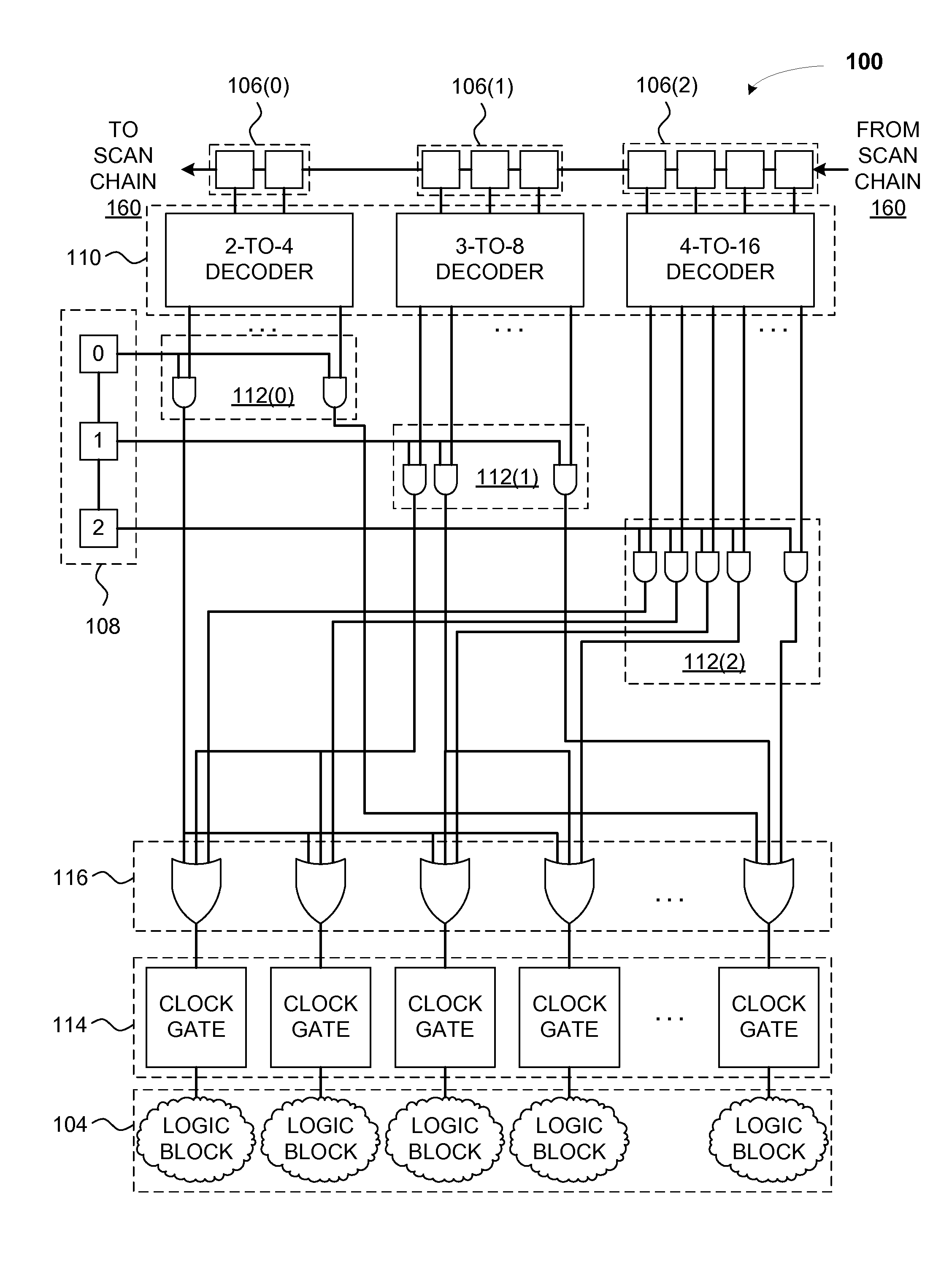
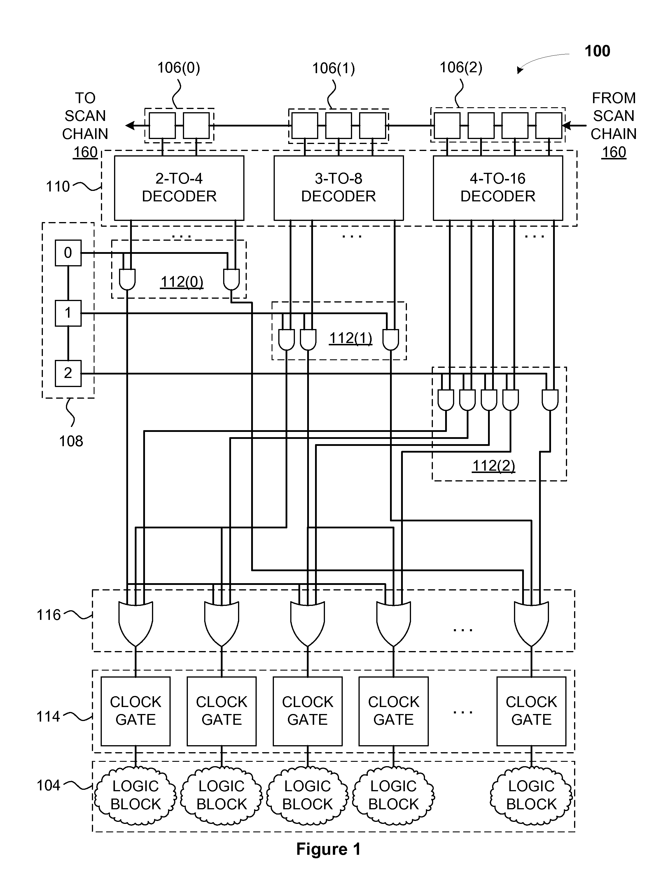
[0020]FIG. 1 illustrates a clock gating mechanism 100 configured to control power in an integrated circuit device under test (DUT), according to one embodiment of the present invention. As shown, the clock gating mechanism 100 includes selector flip-flops 106, a decoder tree 110, level controls 112, control bits 108, OR gates 116, clock gates 114, and logic blocks 104.

[0021]The selector flip-flops 106 form binary input codes that select which decoder outputs in the decoder tree 110 are active. As shown, the selector flip-flops 106 are grouped to provide inputs for the multiple decoders in the decoder tree 110. Selector flip-flops 106(0), therefore, provide two inputs for the 2-to-4 decoder within de...


PUM


Abstract

A clock gating mechanism controls power within an integrated circuit device. One or more clock gating circuits are configured to couple a system clock to a different portion of the integrated circuit device. A logic circuit applies an enabling signal to one of the clock gating circuits to control whether the system clock passes through the clock gating circuit to a portion of the integrated circuit device associated with the clock gating circuit. A plurality of scan flip-flops is configured to provide a binary code to the logic circuit, where the binary code indicates to the logic circuit that the enabling signal should be applied to the clock gating circuit. One advantage of the disclosed technique is that power droop during at-speed testing of a device is reduced without significantly increasing the quantity of test vectors or reducing test coverage, resulting in greater test yields and lower test times.

Description

BACKGROUND OF THE INVENTION[0001]1. Field of the Invention[0002]The present invention generally relates to automated testing of integrated circuits and, more specifically, to power droop reduction via clock gating for at-speed scan testing.[0003]2. Description of the Related Art[0004]As transistor geometries decrease in size and integrated circuit device surface areas increase, the number of transistors per device increases dramatically. Automatic test pattern generation (ATPG) testing of such a device during the manufacturing process typically employs two phases. The first phase (referred to herein as the “scan-load phase”) is used to initialize the device to a known state for a particular test cycle. During the scan-load phase, relatively few transistors are being switched, and the device enters a quiescent, low-leakage current phase of operation. The second phase (referred to herein as the “capture phase”) sends one or more sets of clock pulses through the device to exercise the ...

Claims


Application Information

Patent Timeline
Patent Type & Authority Applications(United States)
IPC IPC(8): H03K3/027H03K3/00
CPCG01R31/318552G01R31/318575
Inventor SANGHANI, AMITYANG, BO
Owner NVIDIA CORP
Why Eureka
Try Eureka