Probe of cantilevel probe card

A probe card, horizontal technology, used in the field of probe cards, can solve the problems of easy sticking of probes, reduce the utilization rate of test machines, and shorten the life of probes, so as to reduce the frequency of needle cleaning and improve the test yield. , the effect of reducing the cost of testing

Inactive Publication Date: 2009-12-02
IPWORKS TECH CORP
View PDF0 Cites 3 Cited by
  • Summary
  • Abstract
  • Description
  • Claims
  • Application Information

AI Technical Summary

Problems solved by technology

However, although this existing solution has certain effects on the test yield, increasing the contact force will make the probe easily damage the underlying structure of the die to be tested
Especially when introducing fragile low-k dielectrics (low-k dielectrics) materials into advanced wafer process technologies (0.13um, 90nm, 65nm...etc.), this existing solution (ie increased contact force) It is even more difficult to apply this kind of fragile low-k dielectric material to wafer probing and subsequent packaging, because low-k and ultra-low-k materials are used below 0.13um Integrated circuit manufacturing process requires wafer needle testing technology not to cause deformation or damage to low dielectric materials and their underlying materials or structures
In addition, if cleaning probes are used as a solution, the frequency of cleaning probes may increase rapidly due to problems such as an increase in the number of probes or a decrease in the distance between probes. needle life
[0006] The above-mentioned horizontal probe cards generally have the problem that the probes are easy to stick. Although the industry has recently developed a metal coating on the surface of the probes, it can solve the problem of life at most but still cannot solve the problem of sticking the probes. Therefore, Still unable to improve test yield and test stability

Method used


Image

  • Probe of cantilevel probe card
  • Probe of cantilevel probe card

Examples


Embodiment Construction

[0015] Specific embodiments are listed below to describe the content of the present invention in detail, and illustrations are used as auxiliary descriptions.

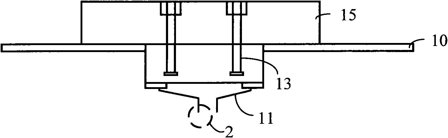
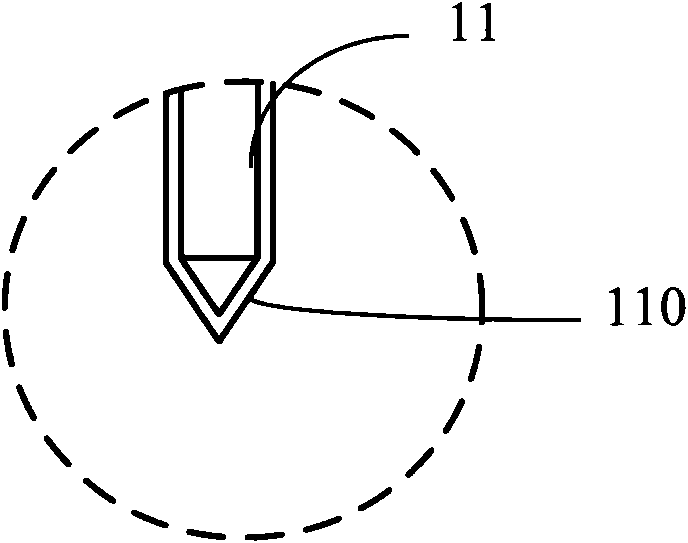
[0016] The invention discloses a horizontal probe card, which includes a plurality of probes and conductive polymer nano-coatings, wherein the probes are made of metal materials and installed on the horizontal probe card, and the conductive polymer nano-coatings are coated on these probes.

[0017] The above-mentioned conductive polymer nano-coating is a conductive polymer material with non-stick properties, such as polypyrrole, polyparaphenylene, polythiophene, polyaniline or the above-mentioned At least one selected composition or its derivatives in the group, and the thickness of the conductive polymer nano-coating film is, for example, 1-20 nanometers, and can be, for example, 1-5 nanometers.

[0018] The above-mentioned probe is made of a metal material, such as nickel, gold, copper, tungsten, rhenium, titanium, ...


PUM

PropertyMeasurementUnit
thicknessaaaaaaaaaa
thicknessaaaaaaaaaa

Abstract

The invention discloses a probe of a cantilevel probe card (epoxide resin probe card). The technical scheme is achieved as follows: high electroconductive polymer materials, nanometer plating of which is thick in 1-20 nm, are plated on the surface of a probe point far away from 5-10mil about. The nanometer plating of the probe effectively enables the probe to have better qualities of no adhesive, high conductivity, contact force reduction and long service life through the plating process, thereby improving the test yield of washers, lowering the frequency of cleaning the probe and reducing the whole test cost.

Description

technical field [0001] The present invention relates to a probe card (Probe Card) for wafer probe (Wafer Probe), and in particular to a probe of a horizontal probe card with conductive polymer nano-coating film. Background technique [0002] A probe card (Probe Card) is composed of a multi-layer printed circuit board (PCB), some of which have more than 30 layers. The contacts, or pads, where each probe makes contact with the wafer, are far smaller than a hair. Among them, the probe card is used before the integrated circuit (IC) is packaged, and the probe can be used to perform functional tests on the chips (Die) cut from the wafer (Wafer), screen out defective products, and then perform subsequent packaging Engineering, therefore, wafer probing is one of the important processes in integrated circuit manufacturing that has a considerable impact on manufacturing costs. [0003] Because the assembly process of the existing probe card requires a lot of manpower and time, and ...

Claims


Application Information

Patent Timeline
Patent Type & Authority Applications(China)
IPC IPC(8): G01R1/073G01R31/28G01R31/26H01L21/66
Inventor 陈彬龙陈皇志
Owner IPWORKS TECH CORP
Why Eureka
Try Eureka