UV LED with tunnel-injection layer

a technology of ultraviolet light and tunnel injection layer, which is applied in the direction of semiconductor/solid-state device manufacturing, electrical apparatus, and semiconductor devices. it can solve the problems of unwanted parasitic luminescence, low carrier injection rate, and ineffective p-doping of these wavelengths, so as to reduce ancillary luminescence and improve internal and external quantum efficiency.

Active Publication Date: 2013-10-24
FERDINAND BRAUN INST GGMBH LEIBNIZ INST FUR HOCHSTFREQUENZTECHNIK +2
View PDF6 Cites 17 Cited by
  • Summary
  • Abstract
  • Description
  • Claims
  • Application Information

AI Technical Summary

Benefits of technology

[0007]In a first aspect, the invention provides a UV LED structure having a thin injection layer of doped or undoped AlN or AlGaN between the active zone and the p-side of a UV LED, with or without EBL. According to this structure, the carrier injection in the active zone is significantly improved so that the internal and external quantum efficien

Problems solved by technology

This makes effective p-doping for these wavelengths practically impossible.
Therefore the carrier injection is very low and there is the additional problem of unwanted parasitic luminescence.
In addition both the internal and external quantum efficiency of LEDs at these wavelengths are extremely low (between 222-240 nm a fraction of a percent and from 250-280 nm. around one percent) and the performance is extremely low.
For deep UV wavelengths this requires high Al concentrations for the EBL whose p-doping is difficult due to the high ionization energy of the magnesium accep

Method used


Image

  • UV LED with tunnel-injection layer
  • UV LED with tunnel-injection layer
  • UV LED with tunnel-injection layer

Examples


Embodiment Construction

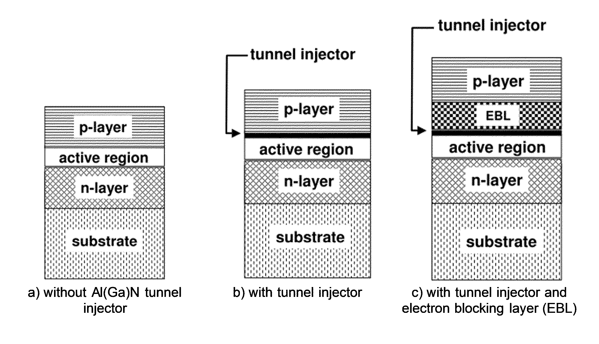
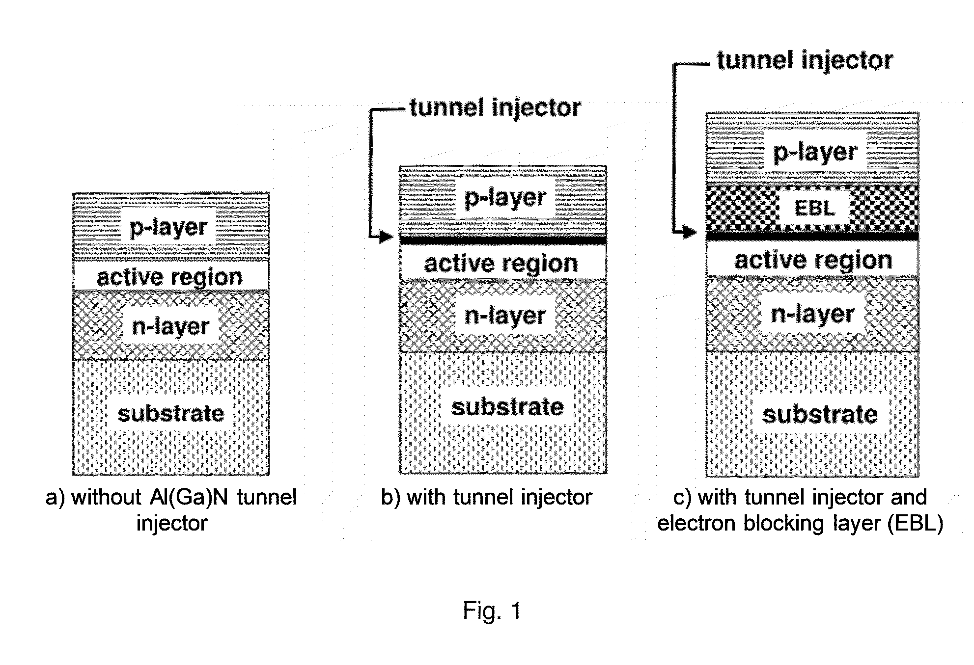
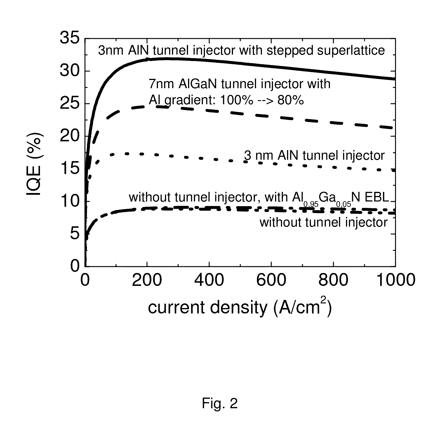
[0018]The invention provides a semiconductor-based ultraviolet (UV) light emitting diode structure having a thin doped or undoped AlN or AlGaN injection layer (with high Aluminum content) between the light emitting active zone and the p-doped layers of a UV LED. In one embodiment, the AlN or AlGaN injection layer is unintentionally doped. In another embodiment, the AlN or AlGaN injection layer is n-doped, e.g., doped with Si, Ge, or O. In preferred embodiments, the AlN or AlGaN injection layer should not be Mg-doped. The inventors have found that the hole injection into the active zone is unexpectedly improved by using the inventive injection layer in semiconductor-based ultraviolet (UV) light emitting diode devices, which greatly improves the external quantum efficiency (EQE) and internal quantum efficiency (IQE). Light emitting heterostructures and LEDs and methods of making such devices and structures are described in U.S. 2010 / 0032647; U.S. Pat. No. 7,977,687; U.S. Pat. No. 7,84...


PUM


Abstract

An ultraviolet (UV) light emitting structure, a UV light emitting device, and a method of making a UV light emitting structure or device, wherein the UV light emitting structure or device has an AlN or AlGaN injection layer with high aluminum content between the light emitting active region and the p-doped layers and wherein the injection layer has a thickness such that holes can tunnel from the p-side of the semiconductor-based ultraviolet light emitting diode structure through the injection layer in the active zone and also reducing leakage electrons out of the active zone.

Description

FIELD OF THE INVENTION[0001]The present invention is an ultraviolet (UV) light emitting structure having a tunnel-injection layer, a UV light emitting device, and a method of making a UV light emitting structure or device.BACKGROUND OF THE INVENTION[0002]Most existing UV light emitting diodes (LEDs) use an electron blocking layer (EBL), which is a ˜15-20 nm, p-doped Mg:AlGaN layer intended to improve hole injection in the active layer as well as to reduce electron leakage current from the active layer. EBLs function quite well for wavelengths >300 nm, but their effectiveness is drastically reduced at shorter wavelengths. This is because at wavelengths <280 nm the barrier layer must carry a high concentration of Al (between 60 and 100%) and the ionization energy of the Mg acceptors is very high. This makes effective p-doping for these wavelengths practically impossible. Therefore the carrier injection is very low and there is the additional problem of unwanted parasitic lumines...

Claims


Application Information

Patent Timeline
IPC IPC(8): H01L33/06
CPCH01L33/06H01L33/32
Inventor KNEISSL, MICHAELKOLBE, TIM
Owner FERDINAND BRAUN INST GGMBH LEIBNIZ INST FUR HOCHSTFREQUENZTECHNIK
Why Eureka
Try Eureka