Light-emitting diode structure and method for manufacturing the same

a technology of light-emitting diodes and led layers, which is applied in the direction of semiconductor/solid-state device manufacturing, electrical apparatus, semiconductor devices, etc., can solve the problems of inability to determine through measurement whether the series led structure b>100/b> has and the need for a short circuit defect is not yet addressed in the art, so as to improve the step coverage capability of the interconnection layer during deposition and reduce the interconnection layer's interconnection layer's interconnection layer ratio ratio

Inactive Publication Date: 2013-11-07
CHI MEI LIGHTING TECH
View PDF0 Cites 27 Cited by
  • Summary
  • Abstract
  • Description
  • Claims
  • Application Information

AI Technical Summary

Benefits of technology

[0013]Accordingly, in one aspect, the present invention is directed to an LED structure and a method for manufacturing the same, where an interconnection layer extends from an exposed portion of a first conductivity type semiconductor layer of one of neighboring LED chips, directly through a side surface of a mesa structure of the other, onto the mesa structure. Therefore, the aspect ratio of the interconnection layer can be reduced greatly, so that the step coverage capability of the interconnection layer during deposition can be improved effectively, thereby solving the disconnection problem of the interconnection layer.

Problems solved by technology

However, since the bottom of the isolation trench 122 of such a conventional series LED structure 100 needs to extend downwards to the surface 104 of the insulating substrate 102, the isolation trench 122 has an excessive aspect ratio (or depth-to width ration), so that the material of the insulating layer 124 is not easily filled in the isolation trench 122, which easily causes discontinuous deposition, resulting in that pores are easily generated in the insulating layer 124.
Moreover, the excessive aspect ratio of the isolation trench 122 also easily causes discontinuous deposition of the interconnection layer 126, which will result in disconnection of the interconnection layer 126.
Therefore, it cannot be determined through measurement whether the series LED structure 100 has a short circuit defect.
Therefore, a heretofore unaddressed need exists in the art to address the aforementioned deficiencies and inadequacies.

Method used


Image

  • Light-emitting diode structure and method for manufacturing the same
  • Light-emitting diode structure and method for manufacturing the same
  • Light-emitting diode structure and method for manufacturing the same

Examples


Embodiment Construction

[0053]The present invention is more particularly described in the following examples that are intended as illustrative only since numerous modifications and variations therein will be apparent to those skilled in the art. Various embodiments of the invention are now described in detail. Referring to the drawings, like numbers indicate like components throughout the views. As used in the description herein and throughout the claims that follow, the meaning of “a”, “an”, and “the” includes plural reference unless the context clearly dictates otherwise. Also, as used in the description herein and throughout the claims that follow, the meaning of “in” includes “in” and “on” unless the context clearly dictates otherwise. Moreover, titles or subtitles may be used in the specification for the convenience of a reader, which shall have no influence on the scope of the present invention.

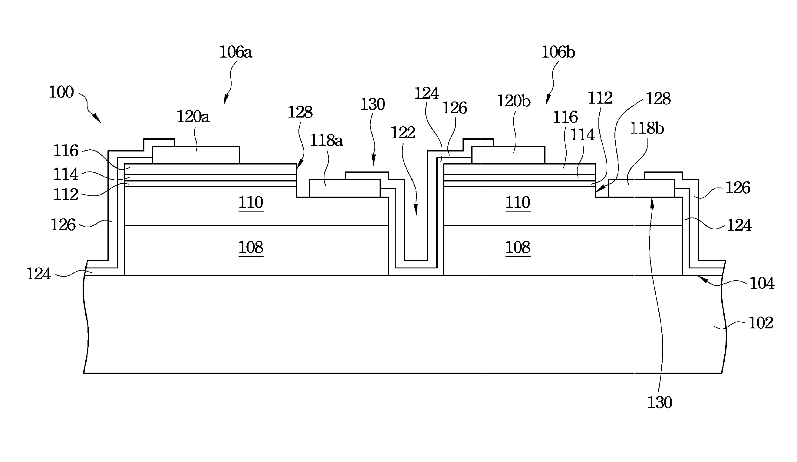
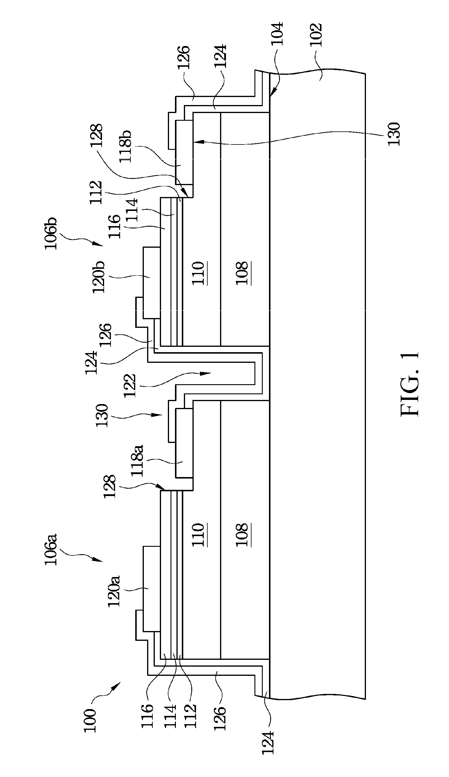
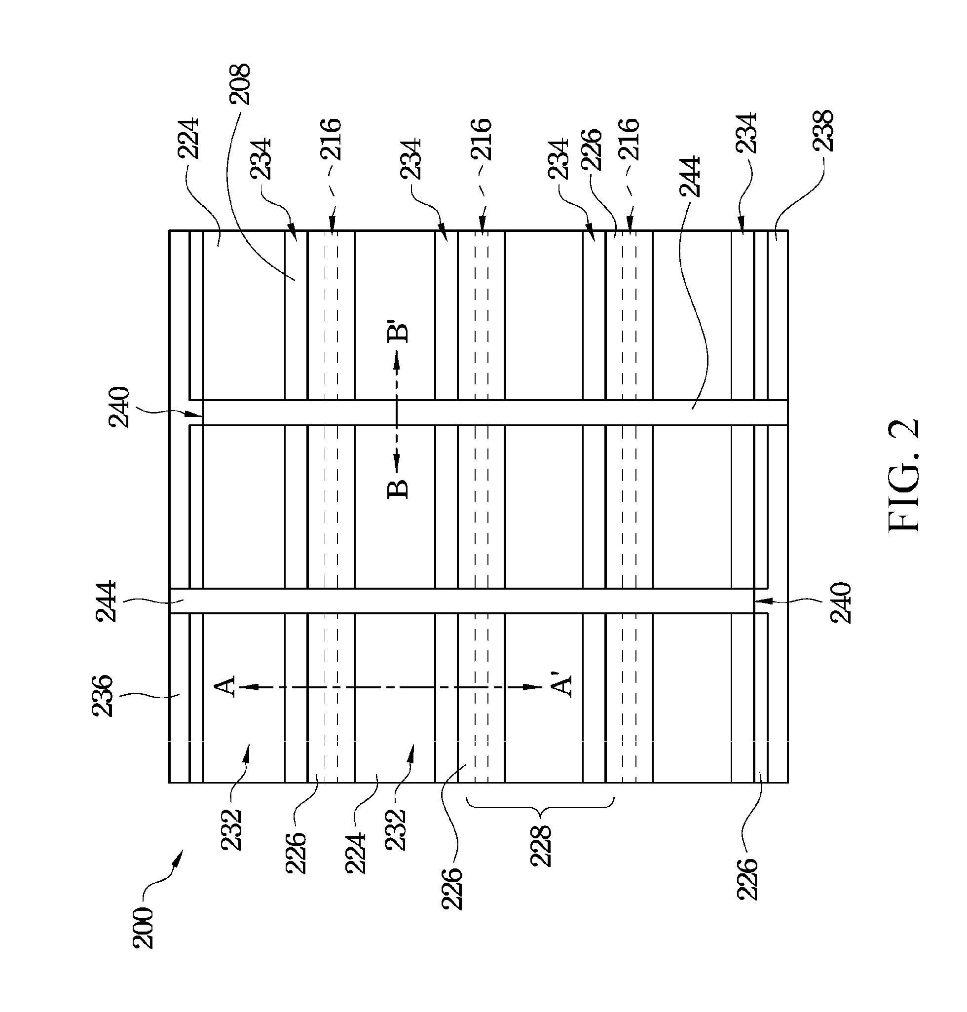
[0054]Referring to FIGS. 2-4, FIG. 2 is a top view of an LED structure according to an embodiment of the pr...


PUM


Abstract

A light-emitting diode (LED) structure and a method for manufacturing the same. The LED structure comprises an insulating substrate, a plurality of LED chips and a plurality of interconnection layers. Each LED chip comprises a first conductivity type semiconductor layer, an active layer and a second conductivity type semiconductor layer stacked in sequence on a surface of the insulating substrate. Each LED chip includes a mesa structure, an exposed portion of the first conductivity type semiconductor layer adjacent to the mesa structure, and a first isolation trench. The first isolation trench is disposed in the mesa structure. The interconnection layers respectively connect neighboring two of the LED chips.

Description

CROSS-REFERENCE TO RELATED APPLICATION[0001]This non-provisional application claims priority under 35 U.S.C. §119(a) on Patent Application No. 101116039 filed in Taiwan R.O.C. on May 4, 2012, the entire contents of which are hereby incorporated by reference.[0002]Some references, if any, which may include patents, patent applications and various publications, may be cited and discussed in the description of this invention. The citation and / or discussion of such references, if any, is provided merely to clarify the description of the present invention and is not an admission that any such reference is “prior art” to the invention described herein. All references listed, cited and / or discussed in this specification are incorporated herein by reference in their entireties and to the same extent as if each reference was individually incorporated by reference.FIELD OF THE INVENTION[0003]The present invention relates to a light-emitting structure, and more particularly to a light-emitting...

Claims


Application Information

Patent Timeline
Patent Type & Authority Applications(United States)
IPC IPC(8): H01L27/15H01L33/36
CPCH01L27/153H01L33/20H01L33/62H01L2924/0002H01L2924/00H01L33/36
Inventor CHU, CHANG HSINLEE, HSUEH LINHSU, CHIH KUEICHEN, YUAN TZE
Owner CHI MEI LIGHTING TECH
Why Eureka
Try Eureka