Semiconductor package integrated with conformal shield and antenna

a technology of conformal shield and semiconductor, applied in the direction of resonant antennas, substantially flat resonant elements, basic electric elements, etc., can solve the problems of high manufacturing cost, easy to occur electromagnetic interference (emi), and difficult to achieve compact product designs

Active Publication Date: 2013-11-07
ADVANCED SEMICON ENG INC
View PDF3 Cites 155 Cited by
  • Summary
  • Abstract
  • Description
  • Claims
  • Application Information

AI Technical Summary

Benefits of technology

[0006]One aspect of the disclosure relates to a semiconductor package. In one embodiment, the semiconductor package comprises a substrate; a semiconductor die disposed on the substrate; a package body encapsulating the semiconductor die; an electromagnetic interference shield formed on the package body; a dielectric structure covering the electromagnetic interference shield; an antenna formed on the dielectric structure; a feeding element connecting the antenna and a feeding point of the substrate; and an antenna grounding element connecting the antenna and the electromagnetic interference shield. In an embodiment the antenna grounding...

Problems solved by technology

Since separate sets of equipment are separately manufactured, higher manufacturing costs are incurred.
Moreover, the conventional approach makes it more difficult to achieve a compact product design.
Furth...

Method used


Image

  • Semiconductor package integrated with conformal shield and antenna
  • Semiconductor package integrated with conformal shield and antenna
  • Semiconductor package integrated with conformal shield and antenna

Examples


Embodiment Construction

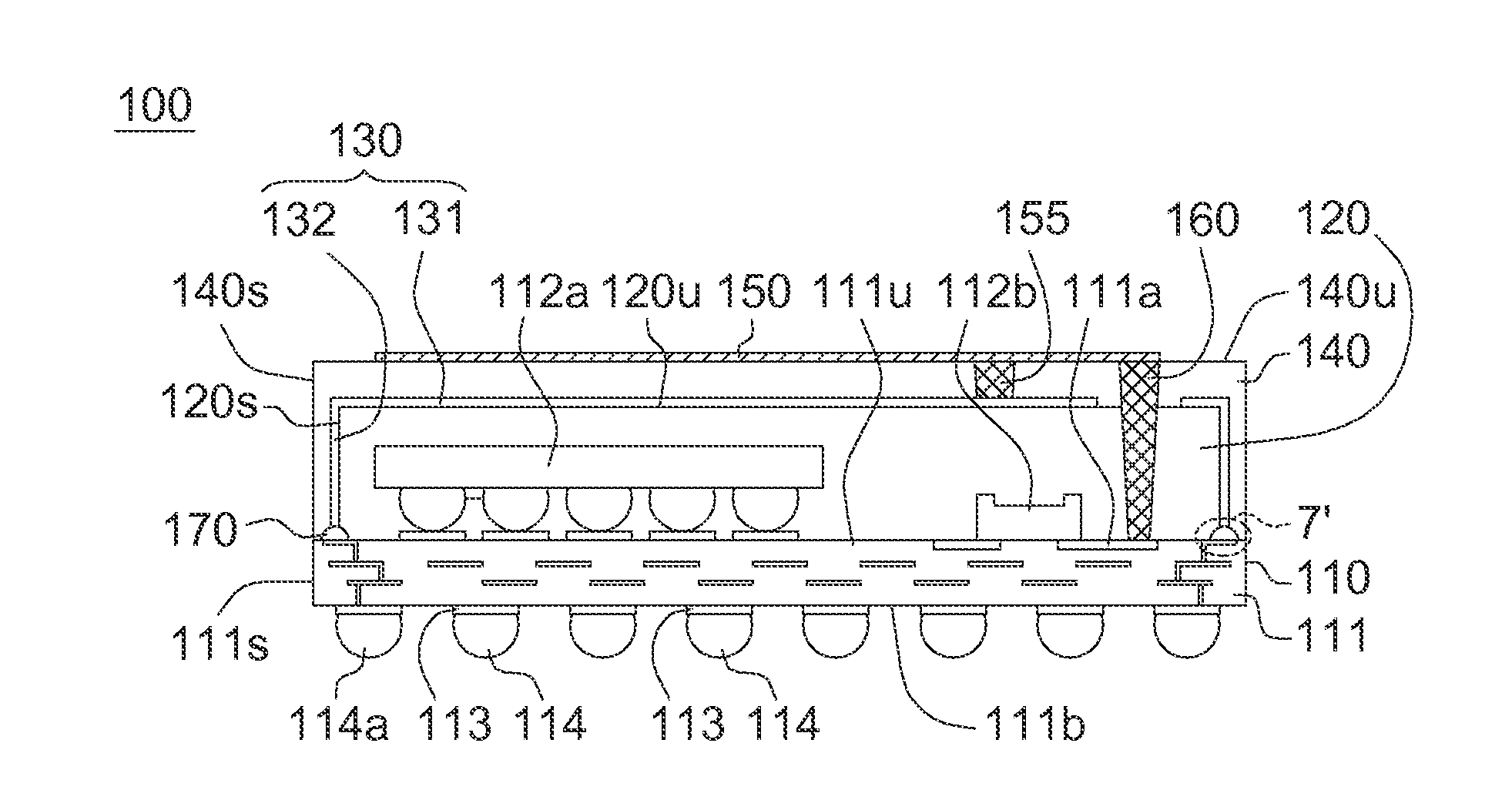
[0036]Referring to FIG. 1 a cross-sectional view of a semiconductor package 100, according to an embodiment of the invention, is illustrated. The semiconductor package 100 includes a, substrate 111, a semiconductor device 112a, a passive element 112b, a package body 120, an electromagnetic interference shielding element 130, a dielectric structure 140, an antenna element 150, a feeding element 160 and an antenna grounding element 155. Advantageously, the semiconductor package 100 of the present embodiment of the invention can be manufactured entirely during a semiconductor packaging process, so that the antenna element 150 is concurrently formed therewith without employing extra antenna manufacturing facilities.

[0037]The substrate 111 includes an upper surface 111u, a lower surface 111b opposite to the upper surface 111u, and a lateral surface 111s at a periphery of the substrate 111. The lateral surface 111s extends between the upper surface 111u and the lower surface 111b, and cir...


PUM


Abstract

A semiconductor package includes a substrate, a semiconductor die, a package body, an electromagnetic interference shield, a dielectric structure and an antenna element. The substrate comprises a grounding segment and a feeding point. The semiconductor die is disposed on the substrate. The package body encapsulates the semiconductor die. The electromagnetic interference shield is formed on the package body. The dielectric structure encapsulates the electromagnetic interference shield. The antenna element is formed on the dielectric structure and electrically connecting the grounding segment of the substrate and the feeding point.

Description

BACKGROUND OF THE INVENTION[0001]1. Field of the Invention[0002]The present invention relates to the field of semiconductor packaging, and, more particularly, to semiconductor packaging in wireless devices.[0003]2. Description of the Related Art[0004]Wireless communication devices, such as cell phones, require antennas for transmitting and receiving signals. Conventionally, a wireless communication device includes therein an antenna and a communication module (e.g., a semiconductor package with RF communication capability), each disposed on different parts of a circuit board. Under the conventional approach, the antenna and the communication module are separately manufactured and electrically connected after being placed on the circuit board. Since separate sets of equipment are separately manufactured, higher manufacturing costs are incurred. Moreover, the conventional approach makes it more difficult to achieve a compact product design.[0005]Furthermore, since antenna signals are ...

Claims


Application Information

Patent Timeline
IPC IPC(8): H01L23/552
CPCH01L23/552H01L24/16H01L24/97H01L2224/16225H01L2924/15311H01L2924/19105H01Q1/2283H01Q9/0407H01Q23/00H01L23/481H01L23/49805H01L21/561H01L23/5389H01L23/3128H01L23/5225H01L23/5227H01L2924/15787H01L2223/6677H01L2224/97H01L2924/15313H01L2924/12042H01L25/16H01L21/568H01L24/19H01L24/96H01L2224/04105H01L2224/12105H01L2924/1815H01L2924/3025H01L2224/05572H01L2924/181H01L2924/00H01L2224/81H01L2924/00012
Inventor YEN, HAN-CHEECHUNG, CHI-SHENGLIAO, KUO-HSIENYEH, YUNG-I
Owner ADVANCED SEMICON ENG INC
Why Eureka
Try Eureka