Hybrid optical modulator

a hybrid optical and modulator technology, applied in the field of optical systems, can solve the problems of reducing device yield, high power consumption, and a variety of performance limitations of current high speed modulators, and achieve the effects of low drive voltage, low insertion loss, and high performan

Active Publication Date: 2013-11-14
SKORPIOS TECH
View PDF5 Cites 38 Cited by
  • Summary
  • Abstract
  • Description
  • Claims
  • Application Information

AI Technical Summary

Benefits of technology

[0015]Numerous benefits are achieved by way of the present invention over conventional techniques. For example, embodiments of the present invention provide a high performance, low drive voltage, low insertion loss, as well as compatibi...

Problems solved by technology

Current high speed modulators suffer from a variety of performance limitations.
These include the need for a high drive voltage, which, in turn, results in high power consumption.
Additionally, conventional high s...

Method used


Image

  • Hybrid optical modulator
  • Hybrid optical modulator
  • Hybrid optical modulator

Examples


Embodiment Construction

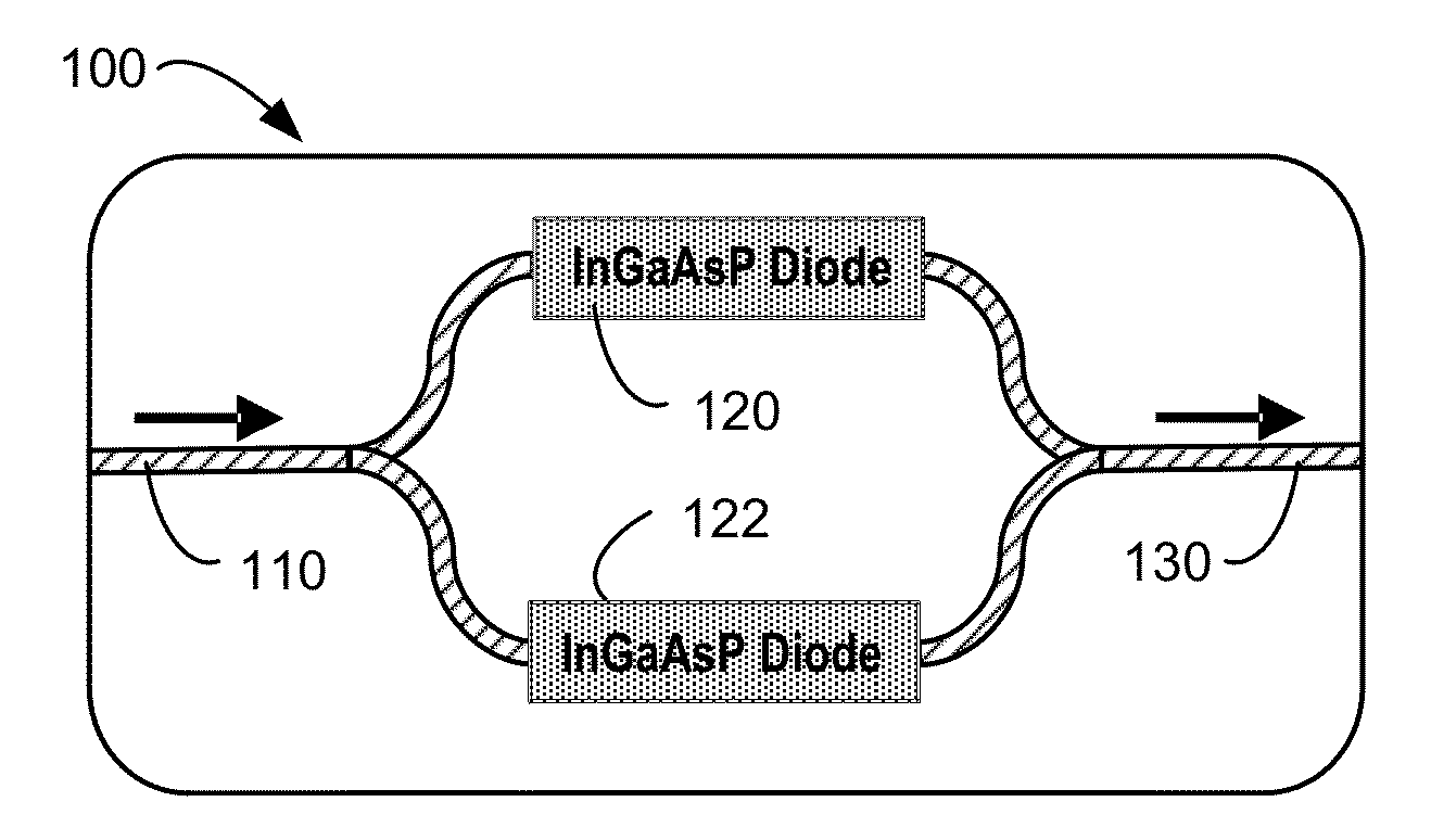
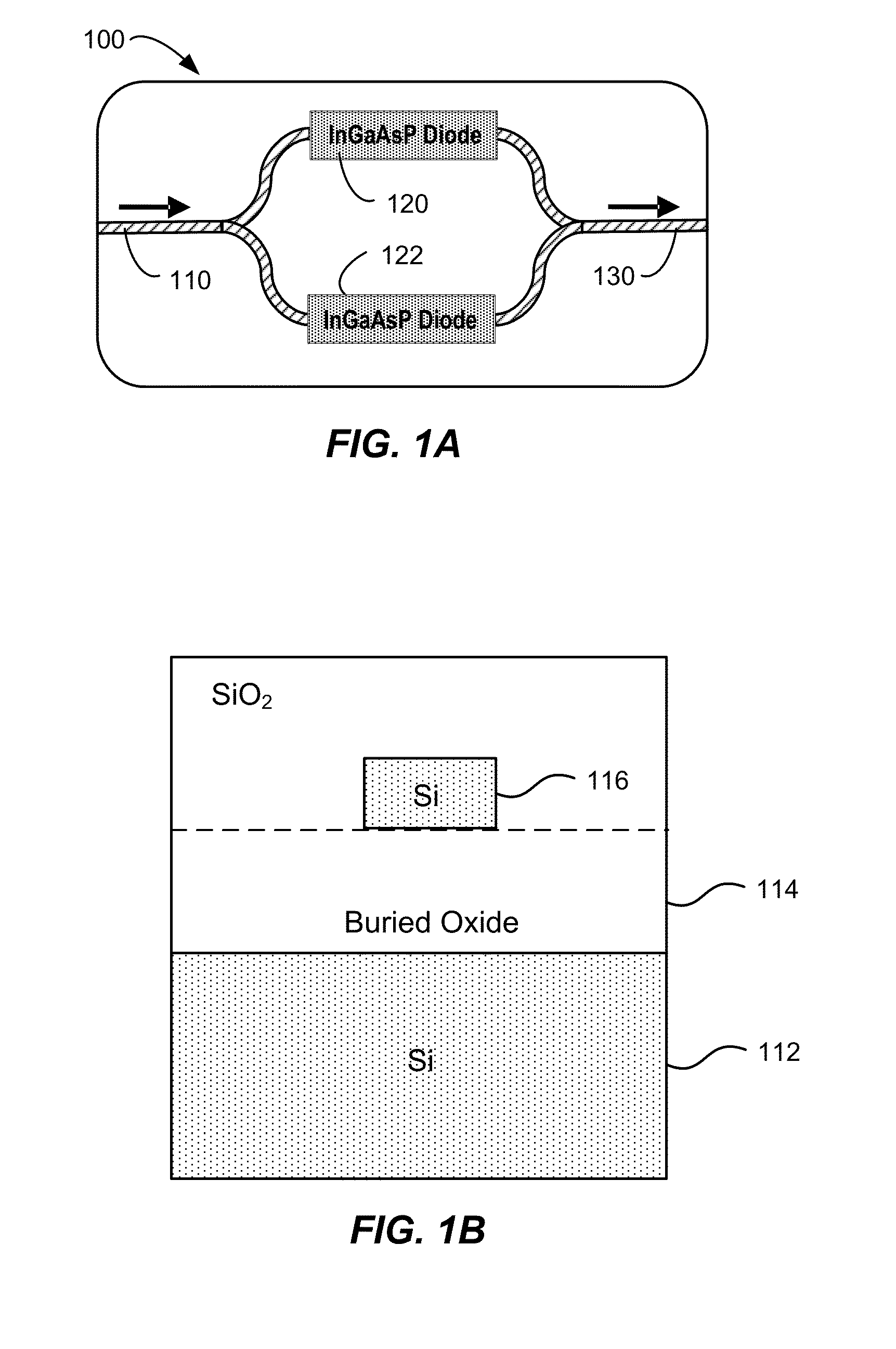
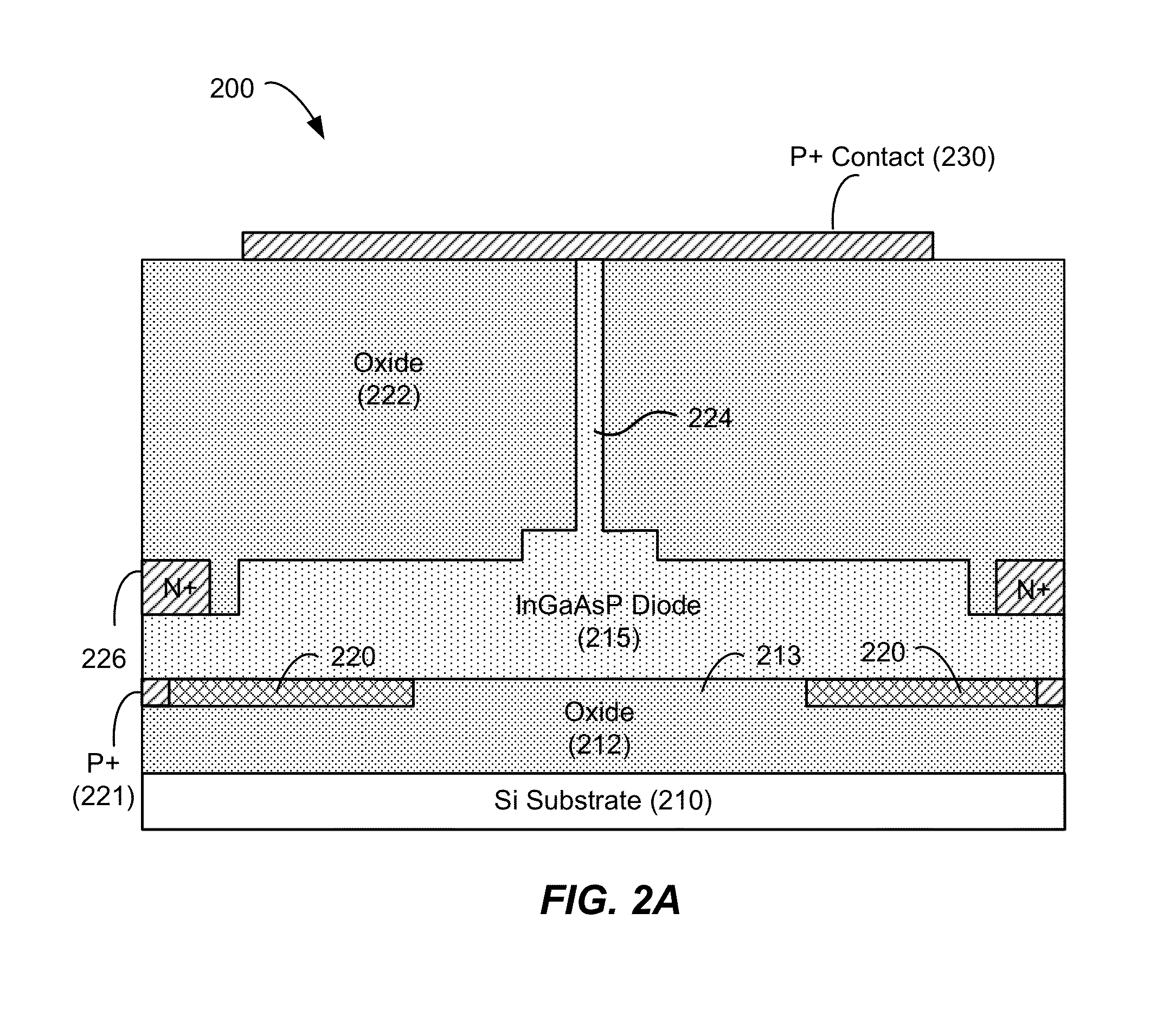
[0025]The inventors have determined that pure silicon modulators suffer from bandwidth limitations, large size, high drive power, and high insertion loss. On the contrary, III-V modulators exhibit higher bandwidth and higher performance than silicon modulators. Although embodiments of the present invention are discussed in terms of Mach-Zehnder modulator (either phase or amplitude modulation) applications, the hybrid diode structure described herein is not limited to these applications, but can also be utilized in other applications including ring modulators, disk modulators, tuning elements based on phase shift, phase bias elements, or other types of phase shifting devices.

[0026]Embodiments of the present invention provide a high-performance hybrid Si / III-V modulator based on a template assisted bonding (TAB) process. The III-V materials are disposed on a low index material, as well as surrounded by low index materials in some implementations.

[0027]High-performance is facilitated b...


PUM


Abstract

An optical modulator includes an input port, a first waveguide region comprising silicon and optically coupled to the input port, and a waveguide splitter optically coupled to the first waveguide region and having a first output and a second output. The optical modulator also includes a first phase adjustment section optically coupled to the first output and comprising a first III-V diode and a second phase adjustment section optically coupled to the second output and comprising a second III-V diode. The optical modulator further includes a waveguide coupler optically coupled to the first phase adjustment section and the second phase adjustment section, a second waveguide region comprising silicon and optically coupled to the waveguide coupler, and an output port optically coupled to the second waveguide region.

Description

CROSS-REFERENCES TO RELATED APPLICATIONS[0001]This application claims priority to U.S. Provisional Patent Application No. 61 / 624,099, filed on Apr. 13, 2012, entitled “Hybrid Optical Modulator,” the disclosure of which is hereby incorporated by reference in its entirety for all purposes.BACKGROUND OF THE INVENTION[0002]High speed modulators are utilized in communications systems to modulate signals, for example, digital signals. High speed modulators using, for example, Mach Zehnder interferometer designs, have been implemented in lithium niobate and InP as discrete components that are utilized in conjunction with discrete optical elements.[0003]Current high speed modulators suffer from a variety of performance limitations. These include the need for a high drive voltage, which, in turn, results in high power consumption. Additionally, conventional high speed modulators occupy a large footprint, reducing device yield and increasing device cost. Moreover, integration with other optic...

Claims


Application Information

Patent Timeline
IPC IPC(8): G02F1/025H01L21/02H01L29/20
CPCG02F1/025H01L29/20H01L21/02538G02F1/2257G02F2202/102G02F2202/105
Inventor SPANN, JOHN Y.VAN ORDEN, DEREKMIZRAHI, AMITCREAZZO, TIMOTHYMARCHENA, ELTONSTONE, ROBERT J.KRASULICK, STEPHEN B.
Owner SKORPIOS TECH
Why Eureka
Try Eureka