Substrate manufacturing method and multi-layer structure

a manufacturing method and flexible display technology, applied in the field of substrate manufacturing methods, can solve the problems of limiting application and use, display parts will be damaged, and the problem of thermal bending is getting serious, and achieve the effects of easy realization, simple mechanism of the adhering machine, and ease of thermal bending

Inactive Publication Date: 2013-11-14
AU OPTRONICS CORP
View PDF6 Cites 2 Cited by
  • Summary
  • Abstract
  • Description
  • Claims
  • Application Information

AI Technical Summary

Benefits of technology

[0010]In order to solve the problems of the prior art, the disclosure provides an improved substrate manufacturing method, in which a transparent substrate and a flexible substrate are adhered to each other by using a single adhesive layer that only has a single material. The adhesive layer between the transparent substrate and the flexible substrate has local differences after processes of the disclosure and thus has at least two kinds of adhesion. The disclosure uses the single adhesive layer, so the problem of thermal bending can be eased. The transparent substrate and the flexible substrate are adhered to each other by

Problems solved by technology

However, the existing liquid crystal displays, plasma display panels, organic electro luminescence displays, etc. are all made of a glass substrate, thereby limiting application and usage thereof due to without flexibility.
If the adhesion between the flexible substrate and the hard substrate is too strong, the display parts will be damaged during the process of de-bonding; and if adhesion between the flexible substrate and the hard substrate is too weak, the de-boding between the flexible substrate and the hard substrate will occurred during the manufacturing processes of the display parts.
However

Method used


Image

  • Substrate manufacturing method and multi-layer structure
  • Substrate manufacturing method and multi-layer structure
  • Substrate manufacturing method and multi-layer structure

Examples


Embodiment Construction

[0035]Reference will now be made in detail to the present embodiments of the disclosure, examples of which are illustrated in the accompanying drawings. Wherever possible, the same reference numbers are used in the drawings and the description to refer to the same or like parts.

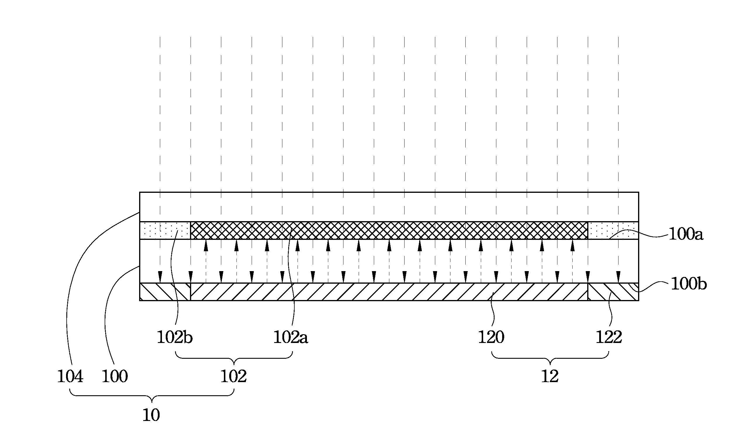
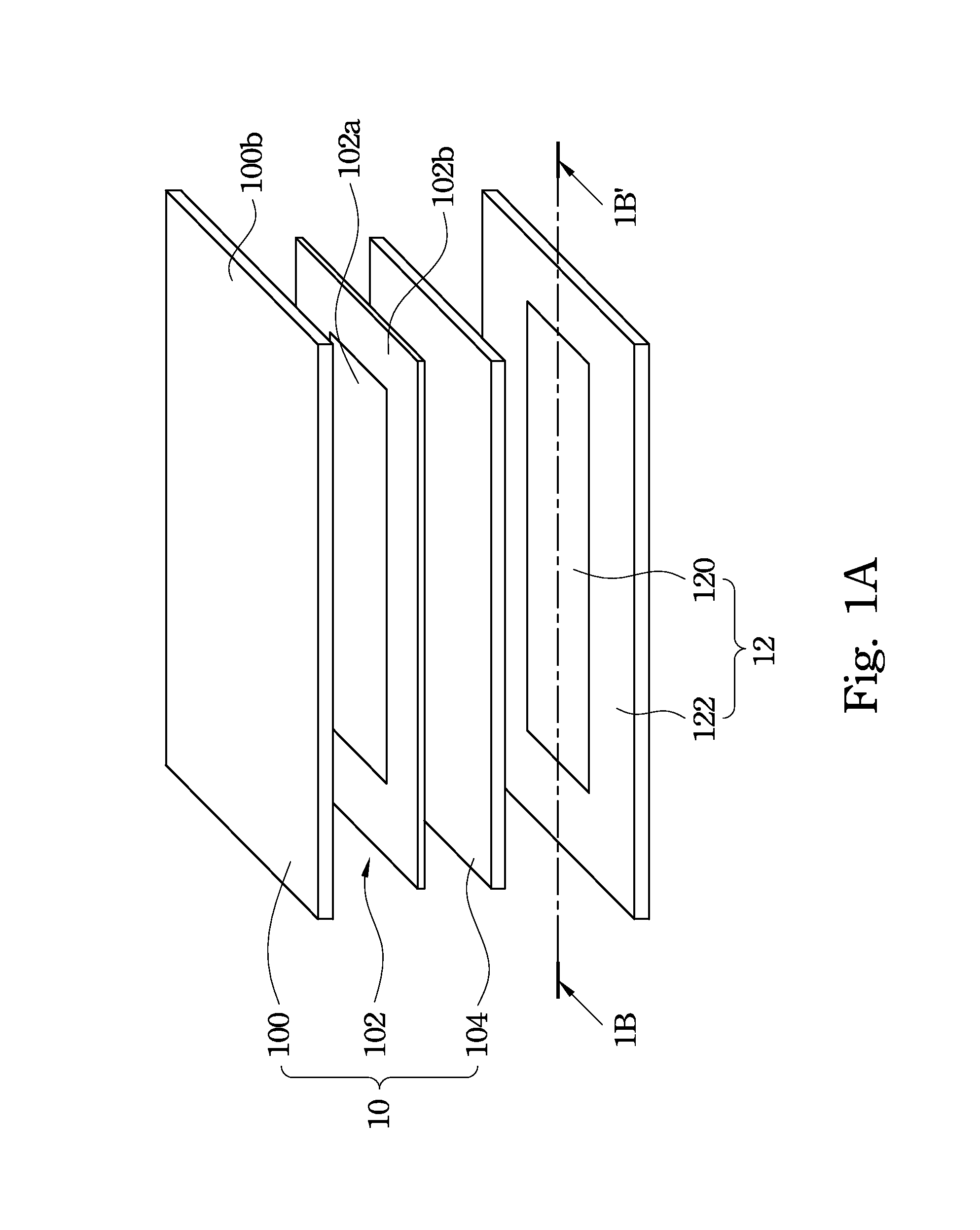
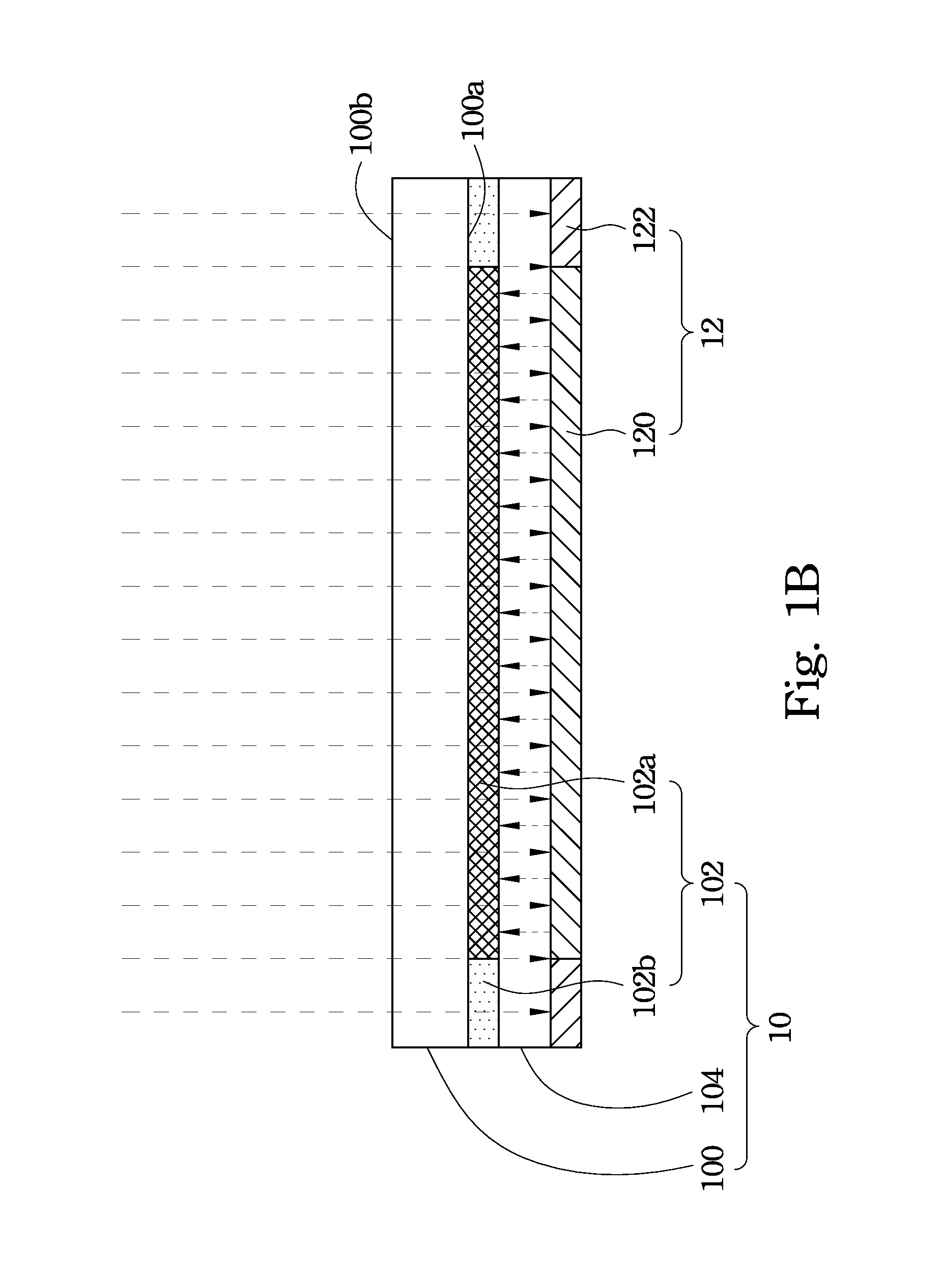
[0036]An improved substrate manufacturing method is provided. Specifically, a transparent substrate and a flexible substrate are adhered to each other by using a single adhesive layer that only has a single material. The adhesive layer between the transparent substrate and the flexible substrate has local differences after processes of the disclosure and thus has at least two kinds of adhesion. The disclosure uses the single adhesive layer, so the problem of thermal bending can be eased. The transparent substrate and the flexible substrate are adhered to each other by the adhesive layer only having the single material, so the process of glue coating can be easily realized, and the mechanism of the used adheri...


PUM

PropertyMeasurementUnit
Structureaaaaaaaaaa
Adhesion strengthaaaaaaaaaa
Flexibilityaaaaaaaaaa

Abstract

A substrate manufacturing method includes steps of: providing a transparent substrate; applying an adhesive layer to a surface of the transparent substrate; disposing a flexible substrate on the adhesive layer to form a multi-layer structure; disposing the multi-layer structure over the reflector, in which the reflector has a first reflecting region and a second reflecting region, and the reflectivity of the first reflecting region is greater than the reflectivity of the second reflecting region; and hardening the adhesive layer by performing an ultraviolet radiation toward the multi-layer structure to form a first hardened portion and a second hardened portion.

Description

RELATED APPLICATIONS[0001]This application claims priority to Taiwan Application Serial Number 101116887, filed May 11, 2012, which is herein incorporated by reference.BACKGROUND[0002]1. Technical Field[0003]The present disclosure relates to a substrate manufacturing method, and more particularly, to a processing method of a flexible display.[0004]2. Description of Related Art[0005]The display device market has been rapidly changing, and flat panel display (FPD) now has become the main stream in the market. The FPD devices can be easily made in a large but thin dimension with lightweight. The FPD devices include liquid crystal displays (LCDs), plasma display panels (PDPs), organic electro luminescence displays (OLEDs), etc. However, the existing liquid crystal displays, plasma display panels, organic electro luminescence displays, etc. are all made of a glass substrate, thereby limiting application and usage thereof due to without flexibility.[0006]Currently, a flexible display devi...

Claims


Application Information

Patent Timeline
IPC IPC(8): B32B37/14B32B7/12
CPCB32B37/144B32B7/12B32B37/12B32B2037/1253B32B2038/0076B32B2310/0831B32B2457/20B32B7/14B32B2307/412B32B2307/416B32B2307/71Y10T428/31504
Inventor WEI, MIN-CHIHWANG, HSIANG-YUNHUANG, TAI-HSIANG
Owner AU OPTRONICS CORP
Why Eureka
Try Eureka